engineered to connect Full Product Line
|
|
|
- Oliver Byrd
- 5 years ago
- Views:
Transcription


1 engineered to connect Full Product Line TEST solutions
2 The technical data and specifications of the products shown in this catalogue are for reference only, and apply to products available at the time of catalogue printing in Nov Product modification often involves changes to technical data and size, and it is therefore recommended that the buyer request the latest technical data and specifications before placing a purchasing contract. Technische Daten und Massangaben der im Katalog aufgeführten Produkte beziehen sich auf Referenzprodukte aus dem Produktsortiment bei Erscheinen des Katalogs im Nov Produktänderungen, insbesondere aufgrund technischer Weiterentwicklung, bedingen regelmäßig veränderte technische Daten und Maße. Dem Besteller wird daher dringend empfohlen, vor Vertragsabschluss technische Daten und Massangaben gesondert nachzufragen.


3 Company Profile Worldwide Yamaichi Electronics, as a supplier of high performance interconnection devices was established 1956 in Tokyo. Yamaichi rapidly achieved world class status as a manufacturer of high quality and reliable components, for use in the most demanding applications of electronic systems, including those with high temperature environments, protected interconnections for harsh environments, high speed interconnections for the Telecom/Datacom infrastructure or robust and long-living solar panel cabling systems. Yamaichi uses state-of-the-art automated production and assembly equipment to produce high precision fine pitch sockets, connectors, cable assemblies and flexible printed circuits with consistent quality and reliability. With nearly 5,000 employees and more than 70,000 m 2 of manufacturing space in Japan, the Philippines, South Korea, China and Germany, Yamaichi can provide its customers with conventional and custom products in the most favorable combination of price, quality and delivery. Europe Yamaichi Electronics Deutschland GmbH is located in Munich and is your European partner for sockets, connectors, cables / assemblies, PCB designs as well as fine pitch flexible printed circuits. Our network includes a knowledgeable and experienced sales staff in Germany, Italy, the UK and France. Also we are supported by a European network of exclusive distributors. (Contact addresses at the end of this catalogue). In order to facilitate the local market demands, Yamaichi has two Design Centers in Munich and Sousse (Tunisia). Our expertise covers the factory automation, wireless communication, telecom/datacom, semiconductor, photovoltaic, medical, automotive and other technologies. Moreover we offer PCB design services as well as cable assemblies from our production facility in Northern Germany. Quality Assurance Yamaichi places great importance on Quality. As the European subsidiary, it is our target to meet the high quality requirements set by the Yamaichi Group. For this reason, we started many years ago with a continuous improvement program. Yamaichi is approved according to the current DIN EN ISO 9001:2008.
4 Table of Contents Contacting - Semiconductor Pin Through Hole Devices SIP (Single Inline Package) 1.27 to 2.0mm pitch, with dual wipe contacts 8 ZIP (Zig-Zag Inline Package) 1.27 to 1.778mm pitch, with dual wipe contacts 9 DIP / SDIP (Dual Inline Package) 2.54mm pitch, for P-DIP and side braze packages 10 Shrink 1.778mm pitch, for HD mounting (SDIP) 11 Shrink 1.778mm pitch, plus piggy-back option (SDIP) 12 PGA / ZIF (Pin Grid Array / Zero Insertion Force) 2.54mm pitch, wiping action system / 2.54mm pitch, wiping action sytem 14 SMT Devices SOJ (Small Outline J-Leads) 1.27mm pitch, dead-bug and live-bug insertion PLCC (Plastic Lead Chip Carrier) 1.27mm pitch, clamshell mm pitch, open top 21 SOP (*Small Outline Packages, Gullwing Leads) Overview Applicable dimensions: 0.4 to 0.5mm pitch / 0.6 / / 0.65 / 0.8 mm pitch / 1.25 / 1.27mm pitch QFP (*Quad Flat Packages, Gullwing Leads) Overview Applicable dimensions: 0.4 to 0.5mm pitch and 0.65mm pitch to 1.0mm pitch LCC (Non-Leaded Devices) and 1.27mm pitch, TH clamshell socket for LCC 35 BGA / CSP / LGA (Ball and Pad Arrays) Overview Applicable dimensions: 0.4 to 0.5mm pitch mm pitch to 0.8mm pitch to 1.27mm pitch Base sockets and full grid sizes for NP Page Numbers by Series QFN (Quad Flat Non-Leaded) Overview Applicable dimensions: 0.4 / 0.5 / 1.00mm pitch IC IC IC51 - PLCC *SOP *QFP TCP/TAB IC53-IC51 LCC IC IC IC IC IC IC IC IC IC IC IC IC IC IC IC IC IC IC IC IC IC IC IC IC IC IC IC IC IC IC IC IC LC NP NP NP NP NP NP NP NP NP NP NP NP NP NP NP NP PS PS PS QFN11T YED , 76 YED YED Y-RED *SOP and QFP variations e.g. TSSOP, BQFP...
5 Table of Contents Contacting - Semiconductor Test Contactors Customised >0.40mm Hinged Type and Volume Test for BGA / CSP / QFN / LGA / QFP / SO Test Contactor - Y-RED Modular Overview 60 >0.40 Hinge Type and Volume Test for BGA / CSP / QFN / LGA 61 Receptacles Design Rules and Ordering Procedure 64 Ordering Codes, Notches and Grooves Guide Post Design 67 Contacting - Semiconductor Spring Probe Pins Overview Contacting - Modules Qseven-Test Adapter Overview 74 ComExpress -Test Adapter Overview 76 Custom-BEC Test Adapter Overview 75 Memory Modules DIMM (Dual Inline Memory Module) 72 Pins Pins Pins and 240 pins Pins , 172 and 200 Pins 85 SIMM (Single Inline Memory Module) 1.27 and 2.54mm pitch, 4 to 100 pins Card Edge Connectors 2.54mm pitch, 180 TH - 40 and 120 pins mm pitch, 180 TH - 28 to 100 pins mm pitch, 180 TH - 36 to 88 pins 92 FPC / FFC Clip Connector Overview 96 TCP / TAB (Tape Packages) 0.25 to 0.5mm pitch, TH clamshell socket and carrier 97 ConTacting - Modules PCB Solutions PCB Solutions PCB Solutions Overview Specialities High-Rel Applications 104 Dockings 104 Semi-Automatic Test Cells 105 Test Fixtures for Automation Industy 105 Reference Pages Examples of QFP and SO pin postions...back pages General Terms of Agreement...back pages Specialities
6
7 Contacting - Semiconductor Pin Through Hole Devices SPECIFICATIONS AND DRAWINGS ARE SUBJECT TO ALTERATION WITHOUT PRIOR NOTICE - DIMENSIONS IN MILLIMETER Contacting - semiconductor 7
8 SEries IC70 Single inline Package (SIP) - TH Specifications Insulation Resistance: Dielectric Withstanding Voltage: Contact Resistance: Current Rating: Operating Temperature Range: Mating Cycles: Materials and Finish Housing: Polysulphone (PSF), glass-filled Contacts: Beryllium Copper (BeCu) Plating: Gold over Nickel Features 1.27 to 1.78mm pitch Dual wipe contacts ensure high reliability Low costs due to selective gold plating 1,000MΩ min. at 500V DC 700V AC for 1 minute 30mΩ max. at 10mA/20mV max. 1A max. 40 C to +150 C 10,000 insertions min. Series No. of Contact Pins Design No. MF = Flanged Unmarked = Not Flanged Contact Plating (G = Gold Plating) Straight, Through Hole Type IC MF - G 4 Outline Socket Dimensions Outline Socket Dimensions for IC G4 only May be cut at points marked by into 3 separate sections Recommended PCB Layout Top View from Socket 1.27 to 1.78mm Pitch Pin Count Pitch A B C D IC **-G x 6 = 7.62 IC **-G x 11 = IC **-G x 14 = IC **-G x 19 = IC **-G x 22 = IC **-G x 23 = IC **-G x 29 = IC **-G x 29 = IC **-G x 29 = IC **-G x 55 = IC **-G x 55 = SPECIFICATIONS AND DRAWINGS ARE SUBJECT TO ALTERATION WITHOUT PRIOR NOTICE - DIMENSIONS IN MILLIMETER Contacting - SemiconduCtor
9 Series IC39 Zig-Zag Inline Package (ZIP) - TH Specifications Insulation Resistance: Dielectric Withstanding Voltage: Contact Resistance: Current Rating: Operating Temperature Range: Mating Cycles: Materials and Finish Housing: Polysulphone (PSF), glass-filled Contacts: Beryllium Copper (BeCu) Plating: Gold over Nickel Features 1.27 to 1.778mm pitch Applicable for Zig-Zag mounted leads Dual wipe contacts ensure high reliability 1,000MΩ min. at 500V DC 700V AC for 1 minute 30mΩ max. at 10mA/20mV max. 1A max. 40 C to +150 C 10,000 insertions min. IC mf - G 4 Series No. of Contact Pins Design No. MF = Flanged Unmarked = Not Flanged Contact Plating (G = Gold Plating) Straight, Through Hole Type Outline Socket Dimensions Recommended PCB Layout A B C D 2- Ø PTH Devices - sip / Zip (contact position) B D H G F Pin Count Ø Ø 2.5 Top View from Socket 0.5 x 0.4 J 1.27 to 1.778mm Pitch Pin Count Pitch A B C D F G H J IC **-G x 11 = IC **-G x 13 = IC **-G x 14 = IC **-G x 15 = IC S**-G x 19 = IC **-G x 22 = IC **-G x 23 = IC **-G x 27 = SPECIFICATIONS AND DRAWINGS ARE SUBJECT TO ALTERATION WITHOUT PRIOR NOTICE - DIMENSIONS IN MILLIMETER Contacting - semiconductor 9
10 SEries IC37 Dual inline Package (DIP) - TH Specifications Insulation Resistance: Dielectric Withstanding Voltage: Contact Resistance: Current Rating: Operating Temperature Range: Mating Cycles: 1,000MΩ min. at 500V DC 700V AC for 1 minute 20mΩ max. at 10mA/20mV max. 1A max. 40 C to +170 C (PPS) 25,000 to 50,000 insertions Materials and Finish Housing: Polyphenylenesulfide (PPS), glass filled Contacts: Beryllium Copper (BeCu) Plating: Gold over Nickel Features 2.54mm pitch Dual wipe contacts ensure high reliability Low costs due to selective gold plating Applicable for IC packages and side braze packages Ideal for automated burn-in IC37N R B G 4 Series No. Housing Material: R = PPS Contact Plating: B = Mating Terminals 0.3µm AU Solder Terminals 0.1µm AU No. of Contacts Row Space (0.3 = 0.3 inches) Gold Plating Straight Through Hole Type Outline Socket Dimensions Recommended PCB Layout 2.4 A B B±0.1 J±0.1 H J ± C D E F G (Contact pos.) G±0.1 Pin Count Top View from Socket 2.54mm Pitch Pin Count A B C D E F G H J IC37NRB-0083-G x 3 = IC37NRB-1403-G x 6 = IC37NRB-1603-G x 7 = IC37NRB-1803-G x 8 = IC37NRB-2003-G x 9 = IC37NRB-2004-G x 9 = IC37NRB-2203-G x 10 = IC37NRB-2204-G x 10 = IC37NRB-2403-G x 11 = IC37NRB-2404-G x 11 = IC37NRB-2406-G x 11 = IC37NRB-2803-G x 13 = IC37NRB-2804-G x 13 = IC37NRB-2806-G x 13 = IC37NRB-3203-G x 15 = IC37NRB-3204-G x 15 = IC37NRB-3206-G x 15 = IC37NRB-4006-G x 19 = IC37NRB-4206-G x 20 = IC37NRB-4806-G x 23 = SPECIFICATIONS AND DRAWINGS ARE SUBJECT TO ALTERATION WITHOUT PRIOR NOTICE - DIMENSIONS IN MILLIMETER Contacting - SemiconduCtor
11 Specifications Insulation Resistance: Dielectric Withstanding Voltage: Contact Resistance: Current Rating: Operating Temperature Range: Mating Cycles: Series IC76 Materials and Finish Housing: Polysulphone (PSF), glass-filled Polyethersulphone (PES), glass-filled Contacts: Beryllium Copper (BeCu) Plating: Gold over Nickel 1,000MΩ min. at 500V DC 700V AC for 1 minute 20mΩ max. at 10mA/20mV max. 1A max. 40 C to +170 C (PES) 25,000 to 50,000 insertions Features Shrink pitch (1.778mm) sockets for high-density mounting Dual wipe contacts ensure high reliability Shrink Dual Inline Package (SDIP) - TH IC76 Series No. Housing Material: 20 = PES No. of Contacts Row Space (0.6 = 0.6 inches) Contact Plating (G = Gold Plating) Straight Through Hole Type MF = Flanged Unmarked = Not Flanged G 4 mf PTH Devices - Dip / SDIP Outline Socket Dimensions Recommended PCB Layout A B H B H Pin Count 0.7 J 1.2 K C Spot facing ( 6.2, 3.0 deep) D (Contact pos.) E F G J G K Top View from Socket mm Pitch Pin Count A B C D E F G H J K IC G4 ** x 9 = IC G4 ** x 10 = IC G4 ** x 11 = IC G4 ** x 13 = IC G4 MF x 14 = IC G4 ** x 19 = IC G4 ** x 20 = IC G4 ** x 23 = IC G4 ** x 25 = IC G4** x 31 = SPECIFICATIONS AND DRAWINGS ARE SUBJECT TO ALTERATION WITHOUT PRIOR NOTICE - DIMENSIONS IN MILLIMETER Contacting - semiconductor 11
, glass-filled Contacts: Copper Alloy Plating: Gold over Nickel 1,000MΩ min. at 500V DC 700V AC for 1 minute 20mΩ max. at 10mA/20mV max.")
12 SEries IC121 Shrink Dual Inline Package (SDIP) - TH Specifications Insulation Resistance: Dielectric Withstanding Voltage: Contact Resistance: Current Rating: Operating Temperature Range: Mating Cycles: Materials and Finish Housing: Polyetherimide (PEI), glass-filled Contacts: Copper Alloy Plating: Gold over Nickel 1,000MΩ min. at 500V DC 700V AC for 1 minute 20mΩ max. at 10mA/20mV max. 1A max. 40 C to +150 C 25,000 to 50,000 insertions Features Shrink pitch (1.778mm) sockets for high-density mounting Dual wipe contacts ensure high reliability Two terminal lengths (3mm / 5mm) available. The 5mm type can be used as a piggy-back socket Series No. No. of Contacts Row Space (0.6 = 0.6 inches) Contact Plating (G = Gold Plating) Straight Solder Dip Terminal Terminal Length Option: L = 5mm Unmarked = Not Flanged MF = Flanged Unmarked = Not Flanged IC G 4 L mf Outline Socket Dimensions Recommended PCB Layout A B R J ±0.1 D ±0.1 J C G F E D 1.2 H K 3.3 Hole 4.0 H ±0.1 B ± ± Top View from Socket 1.778mm Pitch Pin Count A B C D E F G H J K IC G4 ** IC G4 ** IC G4 ** IC G4 ** IC G4 ** IC G IC G4 ** IC G4 ** IC G4 ** SPECIFICATIONS AND DRAWINGS ARE SUBJECT TO ALTERATION WITHOUT PRIOR NOTICE - DIMENSIONS IN MILLIMETER Contacting - SemiconduCtor
 Plating: Gold over Nickel 1,000MΩ min. at 500V DC 700V AC for 1 minute 30mΩ max. at 10mA/20mV max.")
13 Specifications Insulation Resistance: Dielectric Withstanding Voltage: Contact Resistance: Operating Temperature Range: Materials and Finish Housing: Polyetherimide (PEI), glass-filled Contacts: Beryllium Copper (BeCu) Plating: Gold over Nickel 1,000MΩ min. at 500V DC 700V AC for 1 minute 30mΩ max. at 10mA/20mV max. 40 C to +170 C Features Wiping action system: Cleans up IC lead surface during handling action Reliable 3 point contact system Cost performance: Different contact thickness for contact area and terminal area Depopulated versions available Also available with lever on the right hand side, standard type is lever on the left hand side Series np89 Pin Grid Array / Zero Insertion Force (PGA / ZIF) - TH Series No. No. of Contact Pins Design Number MF = Flanged Unmarked = Not Flanged Contact Plating (Gold) Contact Terminal Type NP mf G 4 PTH Devices - sdip / PGA-ziF Outline Socket Dimensions Recommended PCB Layout C A 2.54 B D 7.5 B E 0.55 G B F Lever left hand side (standard) Top View from Socket 2.54mm Pitch Pin Count Grid Size Socket and PCB Dimensions A B C D E F NP **-G x NP **-G x NP **-G x NP **-G x NP **-G x NP **-G x NP **-G x NP **-G x NP **-G x NP **-G x SPECIFICATIONS AND DRAWINGS ARE SUBJECT TO ALTERATION WITHOUT PRIOR NOTICE - DIMENSIONS IN MILLIMETER Contacting - semiconductor 13 G

, glass-filled")

 65.00 max. 0.4±0.1 1.27±0.05 1.27x48=60.96±0.1 1.27x48=60.96±0.1 1.27±0.05 (9.")
14 SEries np236 Pin Grid Array / Zero Insertion Force (Interstitial) - TH Specifications Insulation Resistance: 1,000MΩ min. at 500V DC Dielectric Withstanding Voltage: 700V AC for 1 minute Contact Resistance: 30mΩ max. at 10mA/20mV max. Current Rating: 1A max. Operating Temperature Range: 55 C to +170 C Pin Count: 1020 Materials and Finish Housing: Polyethersulphone (PES), glass-filled Contacts: Beryllium Copper Plating: Gold over Nickel (B-class) Lever Shaft: Stainless Steel NP * Series No. No. of Contact Pins Design Number Contact Style of Matching IC Pin 1 = = Features 1.27mm pitch Outline Socket Dimensions NP * Outline IC Dimensions Recommended PCB Layout Top View from Socket NP * Ø max. (2.03) max. 0.4± ± x48=60.96± x48=60.96± ±0.05 (9.44) ± x48=60.96±0.1 (6.90) 14 SPECIFICATIONS AND DRAWINGS ARE SUBJECT TO ALTERATION WITHOUT PRIOR NOTICE - DIMENSIONS IN MILLIMETER Contacting - SemiconduCtor
15
16
17 Contacting - Semiconductor SMT Devices
18 SEries IC100 Small Outline J-Lead (Dead Bug Insertion) 1.27mm Pitch - TH Specifications Insulation Resistance: Dielectric Withstanding Voltage: Contact Resistance: Current Rating: Operating Temperature Range: Mating Cycles: Materials and Finish Housing: Polyetherimide (PEI), glass-filled Contacts: Beryllium Copper (BeCu) Plating: Gold over Nickel 1,000MΩ min. at 500V DC 700V AC for 1 minute 30mΩ max. at 10mA/20mV max. 1A max. 55 C to +170 C 10,000 insertions min. Features For inserting SOJ packages in Dead-bug orientation Outstanding durability with low insertion withdrawal force Guides for automated operation The larger contact area and two-point contact design ensures high contact reliability Series No. No. of Contact Pins Row Space (03 = 300ML) (04 = 400ML) IC ** mf G Please specify the number of contacts if a depopulated version is required MF = Flanged Unmarked = Not Flanged Contact Plating Specification Outline Socket Dimensions Recommended PCB Layout 1.27 A Pattern I Pattern II B Orientation of Applicable IC (Dead Bug) Pin No1 D±0.1 # Pin Count 0.8 Pin No1 D±0.1 # Pin Count H E±0.1 G± ±0.05 E±0.1 G± ± ± F± F± ± X 0.25 Top View from Socket 1.27mm Pitch *) Flange not available Row Spacing Pin Count Socket Dim. PCB Dimensions A B D E F G Pattern IC **xx-G 300 mil x 9 = II 8.4 *IC **-G 300 mil x 11 = I 8.4 *IC G 300 mil x 12 = II 8.4 *IC **-G 300 mil x 12 = II 8.4 *IC **-G 300 mil x 13 = I 8.4 IC **xx-G 300 mil x 15 = I 8.4 IC **xx-G 400 mil x 13 = I 10.9 *IC **-G 400 mil x 15 = I 10.9 IC **xx-G 400 mil x 17 = I 10.9 IC **xx-G 400 mil x 19 = I 10.9 IC **xx-G 400 mil x 20 = II 10.9 IC **xx-G 400 mil x 21 = I 10.9 IC **xx-G 500 mil x 17 = I 13.5 IC Dim. H 18 SPECIFICATIONS AND DRAWINGS ARE SUBJECT TO ALTERATION WITHOUT PRIOR NOTICE - DIMENSIONS IN MILLIMETER Contacting - SemiconduCtor
19 Series IC107 Small Outline J-Lead (Live Bug Insertion) 1.27mm Pitch - TH Specifications Insulation Resistance: Dielectric Withstanding Voltage: Contact Resistance: Current Rating: Operating Temperature Range: Mating Cycles: Materials and Finish Housing: Polyetherimide (PEI), glass-filled Contacts: Beryllium Copper (BeCu) Plating: Gold over Nickel 1,000MΩ min. at 500V DC 700V AC for 1 minute 30mΩ max. at 10mA/20mV max. 1A max. 55 C to +170 C 10,000 insertions min. Features For inserting SOJ packages in Live-bug orientation Outstanding durability with low insertion withdrawal force Guides for automated operation The larger contact area and two-point contact design ensures high contact reliability Series No. No. of Contact Pins Row Space (03 = 300ML) (04 = 400ML) IC ** mf G Please specify the number of contacts if a depopulated version is required MF = Flanged Unmarked = Not Flanged Contact Plating Specification SMT DEVICES - SOJ Outline Socket Dimensions Recommended PCB Layout 1.27 A Pattern I Pattern II B Orientation of Applicable IC (Live Bug) Pin No1 D±0.1 # Pin Count 0.8 Pin No1 D±0.1 # Pin Count H E±0.1 G± ±0.05 E±0.1 G± ± ± F± F± ± X 0.25 Top View from Socket 1.27mm Pitch 1) Flange not available Row Spacing Pin Count Socket Dim. PCB Dimensions A B D E F G Pattern IC **xx-G 300 mil x 11 = I 8.4 IC xx-G 300 mil x 12 = II 8.4 IC **xx-G 300 mil x 13 = I 8.4 IC **xx-G 300 mil x 15 = I 8.4 IC **-G 1) 350 mil x 12 = II 9.7 IC xx-G 400 mil x 13 = I 10.9 IC **xx-G 400 mil x 13 = I 10.9 IC **xx-G 400 mil x 17 = I 10.9 IC **xx-G 400 mil x 19 = I 10.9 IC **xx-G 400 mil x 20 = II 10.9 SPECIFICATIONS AND DRAWINGS ARE SUBJECT TO ALTERATION WITHOUT PRIOR NOTICE - DIMENSIONS IN MILLIMETER Contacting - semiconductor 19 IC Dim. H

20 SEries IC51 Plastic Lead Chip Carrier 1.27mm Pitch (Clamshell) - TH Specifications Insulation Resistance: 1,000MΩ min. at 500V DC Dielectric Withstanding Voltage: 700V AC for 1 minute Contact Resistance: 30mΩ max. at 10mA/20mV max. Current Rating: 1A max. Operating Temperature Range: 55 C to +170 C Mating Cycles: 10,000 insertions min. Materials and Finish Housing: Polyethersulphone (PES), glass-filled Contacts: Beryllium Copper (BeCu) Plating: Gold over Nickel Series No. No. of Contact Pins Number of Sides with Contacts Design Number IC Features Clamshell socket for PLCC packages IC orientation, Live bug Outline Socket Dimensions A C B D Typical PLCC Package 1.27mm Pitch Pin Count A B C (open) D (closed) IC IC IC IC IC IC IC IC IC SPECIFICATIONS AND DRAWINGS ARE SUBJECT TO ALTERATION WITHOUT PRIOR NOTICE - DIMENSIONS IN MILLIMETER Contacting - SemiconduCtor
 - TH Specifications Insulation Resistance: Dielectric Withstanding Voltage: Contact Resistance: Current Rating: Operating Temperature Range: Mating Cycles: 1,000MΩ min.")
 Lower Body:- Polyetherimide (PEI), glass-filled Contacts: Beryllium Copper (BeCu) Plating: Gold over Nickel Features Two-point")
 Outline Socket Dimensions Series No.")
21 Series IC120 Plastic Lead Chip Carrier 1.27mm Pitch (Open Top) - TH Specifications Insulation Resistance: Dielectric Withstanding Voltage: Contact Resistance: Current Rating: Operating Temperature Range: Mating Cycles: 1,000MΩ min. at 500V DC 700V AC for 1 minute 30mΩ max. at 10mA/20mV max. 1A max. 40 C to +170 C 10,000 insertions min. Materials and Finish Housing: Upper Body:- Polyphenylenesulfide (PPS) Lower Body:- Polyetherimide (PEI), glass-filled Contacts: Beryllium Copper (BeCu) Plating: Gold over Nickel Features Two-point contacts and a larger contact width ensures high reliability Auto-ejecting type for automated operation (IC is inserted in one touch operation and pushing the cover raises it for easy IC removal) Available for two types of IC orientation (Live-bug & Dead-bug) Outline Socket Dimensions Series No. No. of Contact Pins Number of Sides with Contacts IC mf Terminal Arrangement and IC Orientation Design Number MF = Flanged Unmarked = Not Flanged Note: Mounting Flange is not available for 18, 20 and IC SMT DEVICES - PLCC 0.35 x 0.25 A C B 1.27mm Pitch Dead Bug *Most compatible socket type Live Bug Inserting Direction of IC DB = Dead-bug LB = Live Bug Pin Count IC Insertion Socket Dimensions A B C *IC LB IC DB *IC DB IC DB *IC DB IC DB IC LB IC DB IC LB *IC DB *IC LB IC DB *IC LB IC DB IC LB *IC DB *IC LB IC DB IC LB IC DB Pin Count IC Insertion Socket Dimensions A B C IC LB *IC DB *IC LB IC DB IC LB IC DB IC LB *IC DB *IC LB *IC DB *IC LB IC DB IC LB *IC DB *IC LB IC LB IC LB *IC LB *IC LB SPECIFICATIONS AND DRAWINGS ARE SUBJECT TO ALTERATION WITHOUT PRIOR NOTICE - DIMENSIONS IN MILLIMETER Contacting - semiconductor 21

22 SEries Overview *SOP (Small Outline Packages, Gullwing Leads) Series IC51 (Clamshell - TH) to 1.27mm Pitch SOP, Tsop Type I & ii Specifications Insulation Resistance: 1,000MΩ min. at 500V DC Dielectric Withstanding Voltage: 700V AC for 1 minute Contact Resistance: 30mΩ max. at 10mA/20mV max. Operating Temperature Range: 40 C to +150 C (for type PSF) 55 C to +170 C (for type PES & PEI) Mating Cycles: 10,000 insertions min. Materials and Finish Housing: Polyetherimide (PEI), glass-filled Contacts: Beryllium Copper (BeCu) Plating: Gold over Nickel Series No. No. of Contact Pins Number of Sides with Contacts Design Number MF = Flanged Unmarked = Not Flanged IC mf Series IC189 (Open Top - TH) to 1.27mm Pitch SOP, Tsop Type I & ii Specifications Insulation Resistance: 1,000MΩ min. at 100V DC, pitch 0.4, 0.5 1,000MΩ min. at 500V DC, pitch 0.65, 0.8,1.27 Dielectric Withstanding Voltage: 100V AC for 1 minute, pitch 0.4, V AC for 1 minute, pitch V AC for 1 minute, pitch 0.8, 1.27 Contact Resistance: 30mΩ max. at 10mA/20mV max. Operating Temperature Range: 40 C to +150 C Mating Cycles: 10,000 insertions Contact Force: 20g to 80g per pin Materials and Finish Housing: Polysulphone (PSF), glass-filled Polyethersulphone (PES), glass-filled Polyetherimide (PEI), glass-filled Contacts: Beryllium Copper (BeCu) Plating: Gold over Nickel Series No. No. of Contact Pins Number of Sides with Contacts Design Number Positioning Pin: N = Without Positioning Pin P = With Positioning Pin IC * * Protection Key** K = With Protection Key Unmarked = Without Protectin Key ** Protection Key: Prevents IC from releasing during transportation Series IC235 (Open Top - TH) to 1.27mm Pitch SOP, Tsop Type ii Specifications Insulation Resistance: 1,000MΩ min. at 500V DC Dielectric Withstanding Voltage: 700V AC for 1 minute Contact Resistance: 30mΩ max. at 10mA/20mV max. Operating Temperature Range: 40 C to +150 C Mating Cycles: 10,000 insertions min. Contact Force: 20g to 80g per pin Materials and Finish Housing: Polyetherimide (PEI), glass-filled Contacts: Beryllium Copper (BeCu) Plating: Gold over Nickel Series No. No. of Contact Pins Number of Sides with Contacts Design Number Positioning Pin: N = Without Positioning Pin P = With Positioning Pin IC * 22 SPECIFICATIONS AND DRAWINGS ARE SUBJECT TO ALTERATION WITHOUT PRIOR NOTICE - DIMENSIONS IN MILLIMETER Contacting - SemiconduCtor
 - 0.")
23 Specifications Insulation Resistance: Dielectric Withstanding Voltage: Contact Resistance: Current Rating: Operating Temperature Range: Mating Cycles: Contact Force: SEries Overview Series IC191 (Open Top - TH) mm Pitch Thin Small Outline Package (Tsop Type I) Materials and Finish Housing: Polyetherimide (PEI), glass-filled Contacts: Beryllium Copper (BeCu) Plating: Gold over Nickel 1,000MΩ min. at 500V DC 700V AC for 1 minute 30mΩ max. at 10mA/20mV max. 1A max. 40 C to +170 C 40 C to +150 C (type -004*) 10,000 insertions min. 20g to 80g per pin *SOP (Small Outline Packages, Gullwing Leads) Series No. No. of Contact Pins Number of Sides with Contacts Design Number Positioning Pin: N = Without Positioning Pin Unmarked = With Positioning Pin IC * SMT DEVICES - SOP (Gullwing) Contact Styles Series IC51 Series IC189 / IC191 Series IC235 Specialities Series IC (kelvin) Series IC (two point Contact) *SOP variations e.g. TSSOP... cont d next page SPECIFICATIONS AND DRAWINGS ARE SUBJECT TO ALTERATION WITHOUT PRIOR NOTICE - DIMENSIONS IN MILLIMETER Contacting - semiconductor 23
24 Applicable Dimensions SOP (Small Outline Packages, Gullwing Leads) Clamshell Type Sockets E B IC51 Series D Open Top Type Sockets D D D E E E IC235 Series IC189 Series IC191 Series SO package Type I C A C A Type II C B A A = Body width B = Lid size for IC C = Tip-to-Tip SO package orientation 0.40mm Pitch Pin Count IC Body A IC Socket and Lid Size B (max.) C L = Clamshell, OT = Open Top, S = Seperator, FB = Floating Base IC Tip-to-Tip C Socket Dimensions D x E Package Type IC x 34.0 SOP CL/FB IC x 34.0 SOP CL/FB IC x 34.0 SOP CL/FB IC * x 16.0 TSOP I OT IC x 34.0 SOP CL/FB IC * x 18.0 TSOP I OT IC x 34.0 SOP CL/FB IC x 34.0 SOP CL/FB Note 0.50mm Pitch Pin Count IC Body A IC Socket and Lid Size B (max.) IC Tip-to-Tip C Socket Dimensions D x E Package Type IC x 40.0 TSOP I CL/FB IC x 38.0 SOP CL/FB IC *-* x 16.0 TSOP I OT IC x 33.5 TSOP I CL/FB IC x 44.0 TSOP I CL/FB IC x 39.0 TSOP I CL/FB IC x 38.0 SOP CL/FB IC * x 16.0 TSOP I OT IC *-* x 40.0 TSOP I OT IC x 44.0 TSOP I CL/FB IC x 44.0 TSOP I CL/FB IC * x 20.0 TSOP I OT IC * x 18.0 TSOP I OT IC * x 18.2 SOP OT IC *-* x 20.0 TSOP I OT IC x 44.0 TSOP I CL/FB IC x 38.0 SOP CL/FB IC x 44.0 TSOP I CL/FB IC x 34.0 SOP NO LID IC * x 20.0 TSOP I OT IC * x 40.0 TSOP I OT IC x 38.0 SOP CL/FB IC x 34.0 SOP NO LID Note 24 SPECIFICATIONS AND DRAWINGS ARE SUBJECT TO ALTERATION WITHOUT PRIOR NOTICE - DIMENSIONS IN MILLIMETER Contacting - SemiconduCtor
25 0.55 / 0.6 / 0.635mm Pitch Pin Count IC Body A IC Socket and Lid Size B (max.) IC Tip-to-Tip C Socket Dimensions D x E Package Type IC x 37.0 SOP CL/FB IC x 39.0 SOP CL/FB IC KS x 35.0 SOP CL/S IC x 35.0 SOP CL/S 0.65mm Pitch Applicable Dimensions SOP (Small Outline Packages, Gullwing Leads) Note SMT DEVICES - SOP (Gullwing) Pin Count IC Body A IC Socket and Lid Size B (max.) IC Tip-to-Tip C Socket Dimensions D x E Package Type IC A x 32.0 SOP CL/S IC x 32.0 SOP CL/S IC x 32.0 SOP CL/FB IC x 32.0 SOP CL/S IC KS x 32.0 SOP CL/S IC * x 22.5 SOP OT IC x 32.0 SOP CL/S IC x 32.0 SOP CL/FB IC KS x 32.0 SOP CL/S IC P x 21.5 SOP OT IC x 32.0 SOP CL/S IC x 32.0 SOP CL/FB IC KS x 32.0 SOP CL/S IC x 32.0 SOP CL/S IC x 24.0 SOP OT IC x 32.0 SOP CL/FB IC * x 22.5 SOP OT IC x 32.0 SOP CL/S IC x 32.0 SOP CL/S IC N x 22.5 SOP OT IC x 36.0 SOP CL/S Note 0.80mm Pitch Pin Count IC Body A IC Socket and Lid Size B (max.) IC Tip-to-Tip C Socket Dimensions D x E Package Type IC x 32.4 SOP CL/S IC x 31.5 SOP CL/S IC x 38.5 SOP CL/FB IC x 32.5 SOP CL/S IC x 38.5 SOP FB IC *-* x 25.4 SOP OT IC x 38.0 SOP FB IC x 42.5 SOP FB IC x 36.5 SOP CL/S IC * x 29.8 SOP OT IC * x 29.8 SOP OT IC x 48.5 SOP CL/S IC *-* x SOP OT IC *-* x SOP OT IC *-* x SOP OT IC * x 37.0 SOP OT IC x 42.0 SOP CL/S IC (50) x 36.5 SOP CL/S Note SPECIFICATIONS AND DRAWINGS ARE SUBJECT TO ALTERATION WITHOUT PRIOR NOTICE - DIMENSIONS IN MILLIMETER Contacting - semiconductor 25
26 Applicable Dimensions SOP (Small Outline Packages, Gullwing Leads) Clamshell Type Sockets E B IC51 Series D Open Top Type Sockets D D D E E E IC235 Series IC189 Series IC191 Series SO package Type I C A C A Type II C B A A = Body width B = Lid size for IC C = Tip-to-Tip SO package orientation 1.00mm Pitch Pin Count IC Body A IC Socket and Lid Size B (max.) C L = Clamshell, OT = Open Top, S = Seperator, FB = Floating Base IC Tip-to-Tip C Socket Dimensions D x E Package Type IC x 28.5 SOP CL/S IC x 32.0 SOP CL/S IC x 35.0 SOP CL/S Note 1.25mm Pitch Pin Count IC Body A IC Socket and Lid Size B (max.) IC Tip-to-Tip C Socket Dimensions D x E Package Type IC x 27.5 SOP CL/S Note 1.27mm Pitch Pin Count IC Body A IC Socket and Lid Size B (max.) IC Tip-to-Tip C Socket Dimensions D x E Package Type IC * x 12.0 SOP OT IC x 32.5 SOP CL/FB IC x 30.0 SOP CL/S IC KS x 27.2 SOP CL/S IC x 32.5 SOP CL/FB IC KS x 27.2 SOP CL/S IC KS x 31.5 SOP CL/S IC *-* x 15.8 SOP OT IC *-* x 16.0 SOP OT IC x 32.5 SOP CL/FB IC x 27.2 SOP CL/S IC x 27.2 SOP CL/S IC x 35.0 SOP CL/S IC x 28.5 SOP CL/S IC x 28.5 SOP CL/S IC x 28.5 SOP CL/S IC x 28.5 SOP CL/S IC x 28.5 SOP CL/S IC x 30.5 SOP CL/S IC x 31.5 SOP CL/S IC x 28.5 SOP CL/S Note 26 SPECIFICATIONS AND DRAWINGS ARE SUBJECT TO ALTERATION WITHOUT PRIOR NOTICE - DIMENSIONS IN MILLIMETER Contacting - SemiconduCtor
27 1.27mm Pitch (CONT'D) Applicable Dimensions Pin Count IC Body A IC Socket and Lid Size B (max.) SOP (Small Outline Packages, Gullwing Leads) IC Tip-to-Tip C Socket Dimensions D x E Package Type IC KS x 31.5 SOP CL/S IC x 22.5 SOP OT IC x 32.5 SOP CL/FB IC x 36.5 SOP CL/S IC x 31.5 SOP CL/S IC x 32.0 SOP CL/FB IC x 26.0 SOP CL/S IC KS x 32.0 SOP CL/S IC x 29.0 SOP CL/S IC * x 22.5 SOP OT IC x 32.5 SOP CL/FB IC x 36.5 SOP CL/S IC x 31.5 SOP CL/S IC x 32.0 SOP CL/FB IC x 28.5 SOP CL/S IC x 32.5 SOP CL/S IC x 29.0 SOP CL/S IC x 32.5 SOP CL/FB IC x 35.5 SOP CL/FB IC *.KS x 32.5 SOP CL/S IC * x 22.5 SOP OT IC x 50.0 SOP CL/S IC x 32.5 SOP CL/S IC x 32.5 SOP CL/S IC x 32.5 SOP CL/S IC x 35.5 SOP CL/FB IC x 32.5 SOP CL/S IC x 32.5 SOP CL/S IC *-* x 26.5 SOP OT IC *-* x 27.5 SOP OT IC x 32.5 SOP CL/S IC x 33.0 SOP CL/S IC x 33.0 SOP CL/S IC x 31.5 SOP CL/S IC x 42.5 SOP CL/FB IC x 52.0 SOP CL/S IC x 34.5 SOP CL/S IC * x SOP OT IC x 55.0 SOP CL/S IC x 40.5 SOP CL/FB IC x 55.0 SOP CL/S Note SMT DEVICES - SOP (Gullwing) SPECIFICATIONS AND DRAWINGS ARE SUBJECT TO ALTERATION WITHOUT PRIOR NOTICE - DIMENSIONS IN MILLIMETER Contacting - semiconductor 27
,")
 30mΩ max. at 10mA/20mV max. 40 C to +150 C (for type PEI/PSF) 55 C to +170 C (for type PES) 55 C to +170 C (for type PEI) 10,000 insertions min. Series No.")
28 SEries Overview *QFP (Quad Flat Packages, Gullwing Leads) Series IC51 (Clamshell - TH) mm to 1.27mm Qfp, PQfp, TQfp and MQuad *QFP variations e.g. BQFP... Specifications Insulation Resistance: Dielectric Withstanding Voltage: Contact Resistance: Operating Temperature Range: Mating Cycles: Materials and Finish Housing: Polysulphone (PSF), glass-filled Polyethersulphone (PES), glass-filled Polyetherimide (PEI), glass-filled Contacts: Beryllium Copper (BeCu) Plating: Gold over Nickel 1,000MΩ min. at 100V DC for 1 minute (socket depended) 30mΩ max. at 10mA/20mV max. 40 C to +150 C (for type PEI/PSF) 55 C to +170 C (for type PES) 55 C to +170 C (for type PEI) 10,000 insertions min. Series No. No. of Contact Pins Number of Sides with Contacts Design Number IC As specifications for this product differ by pitch and material-mix, please contact Yamaichi for detailed information. Series IC357 and IC402 (Open Top - TH) mm to 0.8mm Quad Flat Package (Qfp) with 2-Point ContaCT Type Specifications Insulation Resistance: 1,000MΩ min. at 500V DC, pitch 0.4 to 0.8 Dielectric Withstanding Voltage: 100V AC for 1 minute, pitch 0.5 to 0.8 Contact Resistance: 30mΩ max. at 10mA/20mV max. Operating Temperature Range: 40 C to +150 C Mating Cycles: 10,000 insertions min. Contact Force: 20g to 45g per pin Materials and Finish Housing: Polyetherimide (PEI), glass-filled Polyethersulphone (PES) glass-filled Contacts: Beryllium Copper (BeCu) Plating: Gold over Nickel IC * Series No. No. of Contact Pins Number of Sides with Contacts Design Number Positioning Pin: N = Without Positioning Pin P = With Positioning Pin Series IC234 (Open Top - TH) - 0.4mm to 0.8mm Quad Flat Package (Qfp) with shoulder ContaCT Type Specifications Insulation Resistance: 1,000MΩ min. at 100V DC pitch 0.4, 0.5 1,000MΩ min. at 500V DC pitch 0.65, 0.8 Dielectric Withstanding Voltage: 100V AC for 1 minute pitch 0.4, V AC for 1 minute pitch V AC for 1 minute pitch 0.8 Contact Resistance: 30mΩ max. at 10mA/20mV max. Operating Temperature Range: 40 C to +150 C Contact Force: 20g to 80g per pin Mating Cycles: 10,000 insertions min. Materials and Finish Housing: Polyetherimide (PEI), glass-filled Polyethersulphone (PES) glass-filled Contacts: Beryllium Copper (BeCu) Plating: Gold over Nickel IC * Series No. No. of Contact Pins Number of Sides with Contacts Design Number Positioning Pin: N = Without Positioning Pin P = With Positioning Pin K = Protection Key** ** Protection Key: Prevents IC from releasing during transportation 28 SPECIFICATIONS AND DRAWINGS ARE SUBJECT TO ALTERATION WITHOUT PRIOR NOTICE - DIMENSIONS IN MILLIMETER Contacting - SemiconduCtor
 Specifications Insulation Resistance: Dielectric Withstanding Voltage: Contact Resistance: Operating Temperature Range: Contact Force: Mating Cycles: The information")
, glass-filled Beryllium Copper (BeCu) Gold over Nickel 1,000MΩ min. at 500V DC or 1,000MΩ min. at 100V DC 100/500/700V AC for 1 minute 30mΩ max. at 10mA/20mV max.")
29 Series IC200 / IC201 / IC216 / IC217 / IC218 / IC248 (Open Top - TH) mm to 0.80mm Quad Flat Packages (Qfp) Specifications Insulation Resistance: Dielectric Withstanding Voltage: Contact Resistance: Operating Temperature Range: Contact Force: Mating Cycles: The information above is typical for this Series for individual specifications please contact Yamaichi Materials and Finish Housing: Contacts: Plating: SEries Overview Polyetherimide (PEI), glass-filled Polyphenylenesulfide (PPS), glass-filled Beryllium Copper (BeCu) Gold over Nickel 1,000MΩ min. at 500V DC or 1,000MΩ min. at 100V DC 100/500/700V AC for 1 minute 30mΩ max. at 10mA/20mV max. 40 C to +170 C and 40 C to +150 C 20g to 80g per pin 10,000 insertions min. *QFP (Quad flat Packages, Gullwing Leads) Series No. No. of Contact Pins Number of Sides with Contacts Design Number Positioning Pin: N = Without Positioning Pin P = With Positioning Pin IC * - * Protection Key** K = With Protection Key Unmarked = Without Protectin Key ** Protection Key: Prevents IC from releasing during transportation SMT DEVICES - QFP (Gullwing) Series IC500 (Open Top - TH) mm to 0.80mm Quad Flat Package (Qfp) with 2-Point ContaCT Type Specifications Insulation Resistance: 1,000MΩ min. at 100V DC pitch 0.5 1,000MΩ min. at 500V DC pitch 0.65, 0.8 Dielectric Withstanding Voltage: 100V AC for 1 minute pitch V AC for 1 minute pitch V AC for 1 minute pitch 0.8 Contact Resistance: 30mΩ max. at 10mA/20mV max. Operating Temperature Range: 40 C to +150 C Contact Force: 20g to 80g per pin Mating Cycles: 10,000 insertions min. Materials and Finish Housing: Polyetherimide (PEI), glass-filled Polyethersulphone (PES) glass-filled Contacts: Beryllium Copper (BeCu) Plating: Gold over Nickel Series No. No. of Contact Pins Number of Sides with Contacts Design Number Positioning Pin: N = Without Positioning Pin P = With Positioning Pin K = Protection Key** IC * ** Protection Key: Prevents IC from releasing during transportation Contact Styles Series IC51 Series IC357 / IC402 Series IC234 Series IC (kelvin) Series IC2** Series IC500 SPECIFICATIONS AND DRAWINGS ARE SUBJECT TO ALTERATION WITHOUT PRIOR NOTICE - DIMENSIONS IN MILLIMETER Contacting - semiconductor 29
30 Applicable Dimensions QFP (Quad Flat Packages, Gullwing Leads) Outline IC Package Dimensions Outline Open Top Socket Dimensions Outline Clamshell Socket Dimensions C A H H E B D G G E E F 0.40mm Pitch C L = Clamshell, OT = Open Top Pin Count IC Body A x B IC Tip-to-Tip C X D Parallel Clamp E 1/2 IC Height F Socket Dim. G x H IC x x x 32.0 CL IC x x x 30.0 OT IC x x x 32.0 OT IC * x x x 42.5 CL IC * x x x 34.0 OT IC x x x 42.5 CL IC x x x 42.5 CL IC * x x x 34.0 OT IC x x x 34.0 OT IC x x x 34.0 OT IC x x x 42.5 CL IC x x x 42.5 CL IC x x x 42.5 CL IC * ,0 x 16, x x 36.0 OT QFP11T x x x 42.5 CL IC P x x x 44.0 OT IC * ,0 x 20, x x 40.0 OT IC x x x 50.0 CL IC x x x 50.0 CL IC * x x x 44.0 OT IC * x x x 44.0 OT IC x x x 48.0 CL IC x x x 48.0 CL IC * x x x 48.0 OT IC * x x x 48.0 OT IC x x x 62.0 CL IC x x x 62.0 CL IC x x x 62.0 CL IC x x x 62.0 CL Type 0.50mm Pitch Pin Count IC Body A x B IC Tip-to-Tip C X D Parallel Clamp E 1/2 IC Height F Socket Dim. G x H IC x x x 31.0 CL IC * x x x 26.6 OT IC * x x x 26.6 OT IC * x x x 22.0 OT IC x x x 32.0 CL IC x x x 32.0 CL IC * x x x 36.0 OT IC * x x x 28.7 OT IC * x x x 29.6 OT IC * x x x 29.6 OT Type 30 SPECIFICATIONS AND DRAWINGS ARE SUBJECT TO ALTERATION WITHOUT PRIOR NOTICE - DIMENSIONS IN MILLIMETER Contacting - SemiconduCtor
31 0.50mm Pitch (cont d) Pin Count Applicable Dimensions IC Body A x B IC Tip-to-Tip C X D QFP (Quad Flat Packages, Gullwing Leads) Parallel Clamp E 1/2 IC Height F Socket Dim. G x H IC x x x 26.2 OT IC x x x 29.6 OT IC x x x 35.0 CL IC AC x x x 35.0 CL IC *-* x x x 29.0 OT IC * x x x 29.0 OT IC * x x x 31.6 OT IC x x x 29.0 OT IC x x x 29.0 OT IC x x x 37.0 CL IC x x x 37.0 CL IC x x x 37.0 CL IC *-* x x x 31.0 OT IC * x x x 31.0 OT IC * x x x 33.6 OT IC x x x 31.9 OT IC x x x 31.9 OT IC x x x 31.9 OT IC * x x x 23.8 OT IC x x x 33.6 OT IC x x x 39.0 CL IC x x x 39.0 CL IC x x x 39.0 CL IC x x x 39.0 CL IC KS x x x 39.0 CL IC * x x x 35.6 OT IC x x x 43.0 CL IC KS x x x 36.7 OT IC *-* x x x 43.4 OT IC * x x x 37.0 OT IC x x x 39.6 OT IC x x x x 43.0 CL IC x x x x 43.0 CL IC x x x x 43.0 CL IC * x x x 37.0 OT IC * x x x 37.0 OT IC * x x OT IC * x x x 37.0 OT IC * x x x 30.0 OT IC P x x x 37.0 OT IC x x x 47.0 CL IC x x x 47.0 CL IC x x x 50.0 CL IC x x x 46.0 OT IC * x x x 46.0 OT IC * x x x 46.0 OT IC * x x x 46.0 OT IC x x x 41.0 OT IC x x x 36.0 OT IC x x x 41.0 OT IC x x x 41.0 OT IC x x x 50.0 CL IC x x x 50.0 CL IC x x x 50.0 CL IC *-* x x x 52.2 OT IC *-* x x x 50.6 OT IC *-* x x x 45.0 OT IC * x x x 45.6 OT IC x x x 45.0 OT Type SMT DEVICES - QFP (Gullwing) cont d next page SPECIFICATIONS AND DRAWINGS ARE SUBJECT TO ALTERATION WITHOUT PRIOR NOTICE - DIMENSIONS IN MILLIMETER Contacting - semiconductor 31
32 Applicable Dimensions QFP (Quad Flat Packages, Gullwing Leads) Outline IC Package Dimensions Outline Open Top Socket Dimensions Outline Clamshell Socket Dimensions C A H H E B D G G E E F 0.50mm Pitch (cont'd) Pin Count IC Body A x B IC Tip-to-Tip C X D Parallel Clamp E 1/2 IC Height F Socket Dim. G x H IC P x x x 45.6 OT IC * x x 58.0 CL IC x x x 58.0 CL IC x x x 58.0 CL IC x x x 58.0 CL IC x x x 58.0 CL IC x x x 58.0 CL IC x x x 58.0 CL IC x x x 58.0 CL IC x x x 58.0 CL IC * x x x 56.1 OT IC * x x x 51.6 OT IC x x x 62.0 CL IC *-* x x x 57.6 OT IC x x x 72.0 CL IC x x x 57.6 OT IC x x x 72.0 CL IC x x x 72.0 CL Type 0.635mm Pitch Pin Count IC Body A x B IC Tip-to-Tip C X D Parallel Clamp E 1/2 IC Height F Socket Dim. G x H IC x 22x x x 34.0 OT IC *-* x x x 47.4 OT IC x x x 40.0 OT IC x x x 83.0 OT Type 0.65mm Pitch Pin Count IC Body A x B IC Tip-to-Tip C X D Parallel Clamp E 1/2 IC Height F Socket Dim. G x H IC x x x 34.5 CL QFP11T A102221* x x x 37.0 CL IC * x x x 29.3 OT IC x x x 35.5 CL IC x x x 29.0 OT IC x x x 39.0 CL IC x x x 42.0 CL IC x x x x 41.0 CL IC *-* x x x 38.9 OT IC *-* x x x 32.2 OT Type 32 SPECIFICATIONS AND DRAWINGS ARE SUBJECT TO ALTERATION WITHOUT PRIOR NOTICE - DIMENSIONS IN MILLIMETER Contacting - SemiconduCtor
33 0.65mm Pitch (cont d) Applicable Dimensions Pin Count IC Body A x B IC Tip-to-Tip C X D QFP (Quad Flat Packages, Gullwing Leads) Parallel Clamp E 1/2 IC Height F Socket Dim. G x H IC * x x x 32.2 OT IC x x x 31.9 OT IC x x x 32.2 OT IC x x x 41.0 CL IC x x x 41.0 CL IC x x x 42.5 CL IC KS x x x 41.0 CL QFP11T x x x 39,5 CL IC *-* x x x 38.9 OT IC * x x x 38.2 OT IC * x x x 37.0 OT IC * x x x 37.0 OT IC * x x x 38.2 OT IC * x x x 38.2 OT IC * x x x 38.2 OT IC * x x x 38.2 OT IC * x x x 38.2 OT IC * x x x 38.2 OT IC * x x x 38.2 OT IC x x x x 42.5 CL IC x x x x 42.5 CL IC x x x x 42.5 CL IC x x x x 42.5 CL IC KS x x x x 42.5 CL IC * x x x 38.2 OT IC x x x 38.2 OT IC x x x 42.5 CL IC YED x x x 42.5 CL IC AC x x x 46.2 OT IC x x x 57.0 CL IC x x x 57.0 CL IC *-* x x x 46.2 OT IC * x x x 47.6 OT IC * x x x 47.6 OT IC x x x 57.0 CL IC x x x 57.0 CL IC x x x 57.0 CL IC x x x 57.0 CL IC x x x 57.0 CL Type SMT DEVICES - QFP (Gullwing) 0.80mm Pitch Pin Count IC Body A x B IC Tip-to-Tip C X D Parallel Clamp E 1/2 IC Height F Socket Dim. G x H IC * x x x 26.6 OT IC x x x 35.5 CL IC x x x 37.5 CL IC * x x x 29.6 OT IC * x x x 29.5 OT IC * x x x 27.0 OT IC x x x 40.0 CL IC x x x 40.0 CL QFP11T x x x 35.0 CL IC x x x 40.0 CL IC x x x 40.0 CL IC AC x x x 37.5 CL IC KS x x x 37.5 CL IC KS x x x 40.0 CL IC KS x x x 39.0 CL Type cont d next page SPECIFICATIONS AND DRAWINGS ARE SUBJECT TO ALTERATION WITHOUT PRIOR NOTICE - DIMENSIONS IN MILLIMETER Contacting - semiconductor 33
34 Applicable Dimensions QFP (Quad Flat Packages, Gullwing Leads) Outline IC Package Dimensions Outline Open Top Socket Dimensions Outline Clamshell Socket Dimensions C A H H E B D G G E E F 0.80mm Pitch (cont d) 34 Pin Count Pin Count IC Body A x B IC Body A x B IC Tip-to-Tip C X D IC Tip-to-Tip C X D Parallel Clamp E Parallel Clamp E 1/2 IC Height F SPECIFICATIONS AND DRAWINGS ARE SUBJECT TO ALTERATION WITHOUT PRIOR NOTICE - DIMENSIONS IN MILLIMETER 1/2 IC Height F Socket Dim. G x H IC x x x x 41.0 CL IC x x x 44.0 CL IC x x x 43.0 CL IC * x x x 32.2 OT IC x x x 34.0 CL IC * x x 26.0 CL IC x x x 42.5 CL IC x x x4 2.5 CL IC x x x4 2.5 CL IC x x x 42.5 CL IC *-* x x x 36.6 OT IC x x x x 44.5 CL IC * x x x 38.2 OT IC *-* x x x 38.2 OT IC * x x x 29.2 OT IC * x x x 32.2 OT IC x x x x 42.5 CL IC x x x x 42.5 CL IC x x x x 42.5 CL IC x x x x 42.5 CL IC KS x x x x 42.5 CL IC * x x x 46.2 OT IC * x x x 48.4 OT IC x x x 58.0 CL IC x x x 30.6 CL IC *-* x x x 52.0 OT IC x x x 57.0 CL IC AC x x x 34.0 OT IC x x x 57.0 CL IC * x x x 57.0 CL 1.00mm Pitch Socket Dim. G x H IC x x x 42.5 CL IC x x x 42.5 CL IC KS x x x 42.5 CL IC x x x x 42.5 CL IC *-* x x x 38.9 OT IC x x x x 42.5 CL IC x x x x 38.9 CL IC x x x x 42.5 CL IC x x x x 42.5 CL IC x x x x 42.5 CL IC KS x x x x 42.5 CL Type Type Contacting - SemiconduCtor

35 Series IC53 / IC51 LCC (Clamshell - TH) Specifications Insulation Resistance: Withstanding Voltage: Contact Resistance: Current Resistance: Operating Temp.Range: Mating Cycles: 10,000MΩ min. at 100V DC 700V AC for 1 minute 30mΩ max. at 10mA/20mV max. 1A max. 40 C to +150 C 10,000 insertions min. IC Series No. No. of Contact Pins Number of Sides with Contacts Design Number SMT DEVICES - LCC Futher LCC versions are also available. Please contact Yamaichi for more information L T W Recommended PCB Layouts 44 pins IC pins IC pins IC IC-498 AC ± ± ± ± ± ± x10=12.7± ± x11=11.176± ± x11=111.18± ± ± ± ± mm Pitch (40mil) Pin Count IC Dimensions W L T Contact Position IC ~ ~ ~ x 13.2 PSF Socket Material 1.27mm Pitch Pin Count IC Dimensions W L T Contact Position Socket Material IC ~ ~ ~ ~ 15.4 PES IC ~ ~ ~ ~ 23.0 PES IC AC ~ ~ ~ ~ 23.0 PES SPECIFICATIONS AND DRAWINGS ARE SUBJECT TO ALTERATION WITHOUT PRIOR NOTICE - DIMENSIONS IN MILLIMETER Contacting - semiconductor 35

 DEtails Please Contact Yamaichi Materials and Finish Housing: Polyetherimide (PEI), glass-filled Polyethersulphone (PES), glass-filled Contacts: Beryllium Copper (BeCu) Plating: Gold over")
36 SEries Overview BGA / CSP / LGA Series np437 / NP481 / IC511 / IC539 (Open top and Clamshell - CMT) mm PiTCH BGA / Csp / lga Specifications Insulation Resistance: Dielectric Withstanding Voltage: Contact Resistance: Operating Temperature Range: Contact Force: Actuation Force: 1,000MΩ min. at 100V DC 100V AC for 1 minute 100mΩ max. at 10mA/20mV max. 40 C to +150 C 58.8mN (6gf) per pin approx. 29.6N (3kg) DEtails Please Contact Yamaichi Materials and Finish Housing: Polyetherimide (PEI), glass-filled Polyethersulphone (PES), glass-filled Contacts: Beryllium Copper (BeCu) Plating: Gold over Nickel Features Compression mount 0.4 to 0.6mm fan-out type Depopulation versions available Series IC398 / IC409 / NP504 / (Open top and Clamshell - CMT) mm PiTCH BGA / Csp / lga Specifications Insulation Resistance: Dielectric Withstanding Voltage: Contact Resistance: Operating Temperature Range: Contact Force: Actuation Force: 1,000MΩ min. at 100V DC 100V AC for 1 minute 100mΩ max. at 10mA/20mV max. 40 C to +150 C 58.8mN (6gf) per pin approx. 29.6N (3kg) DEtails Please Contact Yamaichi Materials and Finish Housing: Polyetherimide (PEI), glass-filled Polyethersulphone (PES), glass-filled Contacts: Beryllium Copper (BeCu) Plating: Gold over Nickel Features Compressed Mount Technology (CMT) Depopulation versions available Series NP383 (Open top - TH) mm PiTCH BGA / Csp Specifications Insulation Resistance: 1,000MΩ min. at 100V DC Dielectric Withstanding Voltage: 100V AC for 1 minute Contact Resistance: 100mΩ max. at 10mA/20mV max. Operating Temperature Range: 40 C to +150 C Contact Force: 10gf per pin approx. Operating Force: 2.2kg ±0.5 Materials and Finish Housing: Polyetherimide (PEI), glass-filled Polyethersulphone (PES), glass-filled Contacts: Beryllium Copper (BeCu) Plating: Gold over Nickel Series No. No. of Contact Pins Design Number Positioning Pin Identification: N = Without Positioning P = With Postioning Pin NP383 - *** * Features 2-point Tweezer Style contact system 36 SPECIFICATIONS AND DRAWINGS ARE SUBJECT TO ALTERATION WITHOUT PRIOR NOTICE - DIMENSIONS IN MILLIMETER Contacting - SemiconduCtor


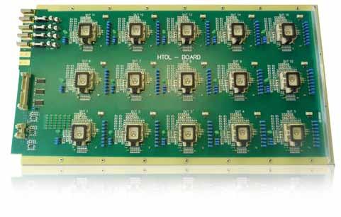
 SMT DEVICES - BGA / CSP / LGA Materials and Finish Housing: Polyetherimide (PEI), glass-filled Polyethersulphone (PES), glass-filled Contacts: Beryllium Copper (BeCu) Plating: Gold over Nickel")
37 SEries Overview BGA / CSP / LGA Series IC280 (Clamshell - TH) mm to 1.00mm PiTCH BGA / Csp / lga Specifications Insulation Resistance: Dielectric Withstanding Voltage: Contact Resistance: Operating Temperature Range: Contact Force: Mating Cycles: 1,000MΩ min. at 100V DC 700V AC for 1 minute for 1.00mmpitch 500V AC for 1 minute for 0.80mm pitch 100V AC for 1 minute for 0.75mm pitch 100mΩ max. at 10mA/20mV max. 40 C to +150 C 15g to 35g per pin within contact travel distance between 0.2 to 0.5mm 10,000 insertions Series No. No. of Contact Pins Design Number For Pin Depopulation and Custom Designed Sockets IC (.AC...) SMT DEVICES - BGA / CSP / LGA Materials and Finish Housing: Polyetherimide (PEI), glass-filled Polyethersulphone (PES), glass-filled Contacts: Beryllium Copper (BeCu) Plating: Gold over Nickel Features V-shape contact structure to lower the damage of coplanarity of solder balls Available in 3 pitch sizes and various depopulation versions, please contact Yamaichi for further available pin counts or custom sockets Series NP291 (Open Top - CMT) mm PiTCH BGA / Csp Specifications Insulation Resistance: Dielectric Withstanding Voltage: Contact Resistance: Operating Temperature Range: Contact Force: Mating Cycles: Materials and Finish Housing: Polyetherimide (PEI), glass-filled Polyethersulphone (PES), glass-filled Contacts: Beryllium Copper (BeCu) Plating: Gold over Nickel 1,000MΩ min. at 100V DC 100V AC for 1 minute 100mΩ max. at 10mA/20mV max. 55 C to +170 C 15g per pin approx. 10,000 insertions Features Contacting structure to nip the sides of solder balls to lower damages of coplanarity of solder balls Series No. No. of Contact Pins Design Number G = Contact Plating (Gold) 4 = Contact Style (180 TH) NP (G4-bf) - * Contact Area - Au (0.3µm min. over Ni) Terminal Area - Au (0.5µm min. over Ni Positioning Pin Identification:: No Mark = Without Positioning Pin "A" and " B" With Mark = For Various Postioning Pin Options (Please Contact Yamaichi) Series NP351 (Open top - TH) mm ptch BGA / Csp / lga Specifications Insulation Resistance: Dielectric Withstanding Voltage: Contact Resistance: Operating Temperature Range: Contact Force: Mating Cycles: Materials and Finish Housing: Polyetherimide (PEI), glass-filled Polyethersulphone (PES), glass-filled Contacts: Beryllium Copper (BeCu) Plating: Gold over Nickel Features Self contacting structure without upper pressing force (ZIF) 2-point Tweezer Style contact system 1,000MΩ min. at 100V DC 100V AC for 1 minute 100mΩ max. at 10mA/20mV max. 55 C to +150 C 15g per pin approx. 10,000 insertions Series No. No. of Contact Pins Design Number H = Also for Handler Use NP (H) - * - (*) Positioning Pin Options Pos. pin "A" Pos. Pin "B" 1 = With With 2 = With Without 3 = Without With 4 = Without Without Contact Terminal Length and Form cont d next page SPECIFICATIONS AND DRAWINGS ARE SUBJECT TO ALTERATION WITHOUT PRIOR NOTICE - DIMENSIONS IN MILLIMETER Contacting - semiconductor 37


 Contacting structure to nip the sides of solder balls to lower damages of coplanarity of solder balls Series np276 (Open top - TH) - 1.")
, glass-filled Polyethersulphone (PES), glass-filled Contacts: Beryllium Copper (BeCu) Plating: Gold over Nickel 1,000MΩ min. at 100V DC 100V AC for 1 minute 100mΩ max.")
 Contacting structure to nip the sides of")
38 SEries Overview BGA / CSP / LGA Series np352 / np483 / np486 (Open top - CMT) mm pitch BGA / Csp Specifications Insulation Resistance: 1,000MΩ min. at 100V DC Dielectric Withstanding Voltage: 100V AC for 1 minute Contact Resistance: 100mΩ max. at 10mA/20mV max. Operating Temperature Range: 55 C to +170 C Contact Force: 15g per pin approx. Mating Cycles: 10,000 insertions Materials and Finish Housing: Polyetherimide (PEI), glass-filled Polyethersulphone (PES), glass-filled Contacts: Beryllium Copper (BeCu) Plating: Gold over Nickel Series No. No. of Contact Pins Design Number NP * - * Mark for Positioning Pin Options (Contact Yamaichi) Contact Terminal Lenght and Form Features Secure package alignment due to self contacting structure without upper pressing force(zif) Contacting structure to nip the sides of solder balls to lower damages of coplanarity of solder balls Series np276 (Open top - TH) mm PiTCH BGA / Csp Specifications Insulation Resistance: Dielectric Withstanding Voltage: Contact Resistance: Operating Temperature Range: Contact Force: Mating Cycles: Materials and Finish Housing: Polyetherimide (PEI), glass-filled Polyethersulphone (PES), glass-filled Contacts: Beryllium Copper (BeCu) Plating: Gold over Nickel 1,000MΩ min. at 100V DC 100V AC for 1 minute 100mΩ max. at 10mA/20mV max. 55 C to +170 C 15g per pin approx. 10,000 insertions Features Open top type sockets for BGA packages Secure package alignment due to self contacting structure without upper pressing force (ZIF) Contacting structure to nip the sides of solder balls to lower damages of coplanarity of solder balls NP * - (*) Series No. No. of Contact Pins (.AC are depopulated base sockets Design No. *Positioning Pin Options Pos. Pin 'A' Pos. Pin 'B' 1 = With With 2 = With Without 3 = Without With 4 = Without Without Contact Terminal Length and Form * for position pin A or B please contact Yamaichi ContaCTing Types For All Series Since the solder balls are touched by two contacts on each side, the solder ball damage can be minimized; additional features are low actuation force and compact socket size U-Shape Style (BGA) Bow Style (LGA) Yamaichi s 2-point Tweezer Style Contact 38 SPECIFICATIONS AND DRAWINGS ARE SUBJECT TO ALTERATION WITHOUT PRIOR NOTICE - DIMENSIONS IN MILLIMETER Contacting - SemiconduCtor
39 Applicable Dimensions BGA / CSP / LGA Typical IC Package Size Outline Socket Dimensions D C A D D SMT DEVICES - BGA / CSP / LGA B C C 0.40mm PiTCH (base Sockets) Pin Count Grid Size Package Size A x B Socket Size C x D IC (max.) up to 22 x 22 up to 11.0 x x 37.0 CL NP (max.) up to 22 x 22 up to 10.0 x x 38.0 OT NP (max.) up to 27 x 27 up to 11.0 x x 40.0 OT IC (max.) up to 28 x 28 up to 12.0 x x 40.0 CL IC (max.) up to 32 x 32 up to 14.0 x x 56.5 CL NP (max.) up to 32 x 32 up to 14.0 x x 45.0 OT Lid Type 0.40mm Pitch Pin Count Grid Size Package Size A x B Socket Size C x D NP x x x 38.0 OT NP x x x 40.0 OT NP x x x 38.0 OT NP x x x 38.0 OT NP x x x 38.0 OT NP x x x 40.0 OT NP x x x 38.0 OT NP x x x 38.0 OT NP x x x 38.0 OT NP x x x 38.0 OT NP x x x 40.0 OT NP x x x 40.0 OT NP x x x 40.0 OT NP x x x 40.0 OT NP x x x 40.0 OT IC x x x 56.5 CL IC x x x 40.0 CL NP x x x 40.0 OT IC x x x 56.5 CL Lid Type 0.50mm PiTCH Pin Count Grid Size Package Size A x B Socket Size C x D IC x x x 38.0 OT IC x x x 38.0 OT IC x x x 38.0 OT IC x x x 32.0 OT IC x x x 38.0 OT IC x x x 37.0 CL NP x x x 26.0 OT IC x x x 37.0 CL IC x x x 38.0 OT IC x x x 38.0 OT IC x x x 38.0 OT Lid Type SPECIFICATIONS AND DRAWINGS ARE SUBJECT TO ALTERATION WITHOUT PRIOR NOTICE - DIMENSIONS IN MILLIMETER Contacting - semiconductor 39
40 Applicable Dimensions BGA / CSP / LGA Typical IC Package Size Outline Socket Dimensions D D A B C C C D 0.50mm PiTCH (cont'd) Pin Count Grid Size Package Size A x B Socket Size C x D IC x x x 32.0 OT IC x x x 32.0 OT IC x x x 38.0 OT NP x x x 32.0 OT NP x x x 26.0 OT IC x x x 32.0 OT NP * x x x 26.0 OT IC x x x 38.0 OT IC x x x 38.0 OT NP x x x 33.0 OT IC x x x 37.0 CL IC x x x 38.0 OT IC x x x 32.0 OT IC x x x 32.0 OT NP *-* x x x 36.0 OT IC x x x 38.0 OT NP * x x x 36.0 OT IC x x x 38.0 OT IC x x x 38.0 OT IC x x x 37.0 CL IC x x x 38.0 OT IC x x x 41.0 OT IC x x x 40.0 OT IC x x x 45.0 OT IC x x x 45.0 OT NP x x x 28.0 OT IC x x x 47.0 CL IC x x x 41.0 OT IC x x x 45.0 OT IC x x x 45.0 OT NP x x x 33.0 OT NP x x x 41.0 OT NP * x x x 33.0 OT Lid Type 0.65mm Pitch Pin Count Grid Size Package Size A x B Socket Dimensions C x D NP *.AC x x x 64.0 OT NP G4-BF-P 48 6 x x x 27.3 OT NP G4-BF-P 48 6 x x x 27.3 OT Lid Type 40 SPECIFICATIONS AND DRAWINGS ARE SUBJECT TO ALTERATION WITHOUT PRIOR NOTICE - DIMENSIONS IN MILLIMETER Contacting - SemiconduCtor
41 0.75mm Pitch Applicable Dimensions Pin Count Grid Size BGA / CSP / LGA Package Size A x B Socket Dimensions C x D NP x x x 20.0 OT NP x x x 20.0 OT NP x x x 20.0 OT NP x 8 6.0x x 20.0 OT NP x x x 26.0 OT NP x x x 20.0 OT NP x x x 20.0 OT NP P 48 6 x x x 20.0 OT NP P x x x 20.0 OT NP x x x 20.0 OT NP x x x 20.0 OT NP P 56 8 x x x 24.4 OT NP P x x 6, x 20.0 OT NP x x x 20.0 OT NP AC x x x 33.9 OT NP G4-BF-P 72 8 x x x 33.9 OT NP AC x x x 33.0 OT NP x x x 33.0 OT IC x x x OT NP x x x 40.0 OT IC x x x 34.6 OT Lid Type SMT DEVICES - BGA / CSP / LGA 0.80mm Pitch Pin Count Grid Size Package Size A X B Socket Dimensions C x D Lid Type NP * 48 8 x x x 36 OT NP * 48 6 x 8 10 x x 33 OT NP * 48 7 x 8 7 x x 33 OT NP " 48 8 x x x 36 OT NP x x x 22 OT NP * x 8 7 x x 25.4 OT NP x 8 7 x x 22 OT NP x 8 10 x x 22 OT NP x x x 22 OT NP x 8 8 x x 22 OT NP x 8 9 x x 22 OT NP * x x x 33 OT NP * 56 8 x 8 7 x x 33 OT NP x 8 11 x x 33 OT NP x 8 11 x x 33 OT NP x x x 25.4 OT NP x x x 22 OT NP x x 22 OT NP * 56 8 x x 33 OT NP x x x 25.4 OT NP AC x 10 9 x 9 36 x 36 OT NP x 8 8 x 8 40 x 40 OT NP * 64 8 x 8 7 x 7 32 x 32 OT NP * 64 8 x 8 8 x 8 36 x 36 OT NP A x 10 9 x 9 36 x 36 OT NP * AC x 12 8 x x 33 OT NP x 10 8 x x 25.4 OT NP * 72 8 x 12 8 x x 25.4 OT NP x 12 8 x x 25.4 OT NP * AC x 12 8 x x 33 OT NP * AC x x x 33 OT NP x 9 8 x 8 18 x 22 OT NP x 8 8 x 8 18 x 22 OT NP x x x 36 OT NP * x 10 9 x 9 36 x 36 OT NP A x x x 36 OT SPECIFICATIONS AND DRAWINGS ARE SUBJECT TO ALTERATION WITHOUT PRIOR NOTICE - DIMENSIONS IN MILLIMETER Contacting - semiconductor 41
42 Applicable Dimensions BGA / CSP / LGA Typical IC Package Size Outline Socket Dimensions D D A B C C C D 0.80mm PiTCH (cont'd) Pin Count Grid Size Package Size A X B Socket Dimensions C x D NP x 10 9 x x 22 OT NP A * x x x 36 OT NP A x 10 9 x 9 36 x 36 OT NP *-* x x x 36 OT NP x x x 36 OT NP * x x x 33 OT NP *-* x x x 36 OT NP * AC x x x 36 OT NP * x x x 36 OT NP * x x x 36 OT NP x x x 24 OT NP * x x x 36 OT NP * x x x 36 OT NP * x x x 33 OT NP x x14 40 x 40 OT NP *-* AC x x x 38 OT NP *-* AC x x x 40 OT NP AC x x13 40 x 40 OT IC x x x CL NP * x x13 38 x 38 OT NP AC x x x 38 OT NP * x x13 38 x 38 OT NP *-1 AC x x x 40 OT NP * x x x 40 OT NP * AC x x13 40 x 40 OT NP * x x13 40 x 40 OT NP *-* x x x 40 OT NP x x x 40 OT NP * x x x 38 OT NP x x x 33 OT IC x x x CS NP x x x 40 OT NP *-* x x x 40 OT NP * x x x 40 OT NP * AC x x x 40 OT NP AC x x x 40 OT NP x x13 40 x 40 OT NP x x x 47 OT NP x x x 38 OT NP x x x 40 OT NP A x x13 38 x 38 OT NP x x x 40 OT NP A x x x 38 OT IC x x x DL NP x x x 40 OT NP * x x x 47 OT NP x x x 40 OT NP A x x x 39 OT NP x x x 40 OT Lid Type 42 SPECIFICATIONS AND DRAWINGS ARE SUBJECT TO ALTERATION WITHOUT PRIOR NOTICE - DIMENSIONS IN MILLIMETER Contacting - SemiconduCtor
43 0.80mm PiTCH (cont'd) Applicable Dimensions Pin Count Grid Size BGA / CSP / LGA Package Size A X B Socket Dimensions C x D NP x x x 40 OT NP *-* x x x 47 OT NP * x x x 47 OT NP * x x x 47 OT NP x x x 47 OT NP x x x 47 OT NP x x x 40 OT NP x x x 47 OT NP x x x 40 OT NP x x x 40 OT IC x x x 47.6 DL Lid Type SMT DEVICES - BGA / CSP / LGA 1.00mm PiTCH Pin Count Grid Size Package Size A X B Socket Dimensions C x D NP x 8 10 x x 28.0 OT NP x 8 11 x x 28.0 OT NP x x 18 26,0 x 22,4 OT NP x x 15 23,6 x 29,9 OT NP x x 17 23,6 x 29,9 OT NP x x 15 31,4 x 34,0 OT NP x x x 39.0 OT NP * x x x 39.0 OT NP x x x 47.0 OT NP x x x 47.0 OT NP x x x 47.0 OT NP x x x 47.0 OT NP AC x x x 62.0 OT NP x x x 62.0 OT NP AC x x x 47.0 OT NP A x x x 62.0 OT NP AC x x x 47.0 OT NP A x x x 62.0 OT NP x x x 47.0 OT NP x x x 62.0 OT NP x x x 62.0 OT NP x x x 47.0 OT NP x x x 47.0 OT NP x x x 62.0 OT NP x x x 62.0 OT NP x x x 62.0 OT NP x x x 62.0 OT NP *-* x x x 47.0 OT NP x x x 62.0 OT NP x x x 47.0 OT NP x x x 47.0 OT NP x x x 47.0 OT NP x x x 47.0 OT NP x x x 47.0 OT NP x x x 47.0 OT NP x x 31 50,0 x 50,0 OT NP AC x x x 62.0 OT NP x x x 47.0 OT NP x x x 62.0 OT NP x x x 47.0 OT NP x x 31 50,0 x 50,0 OT NP AC x x x 62.0 OT IC AC x x x DL NP x x x 47.0 OT NP AC x x x 62.0 OT NP AC x x x 62.0 OT IC x x x DL IC x x x DL NP x x x 62.0 OT Lid Type SPECIFICATIONS AND DRAWINGS ARE SUBJECT TO ALTERATION WITHOUT PRIOR NOTICE - DIMENSIONS IN MILLIMETER Contacting - semiconductor 43
44 Applicable Dimensions BGA / CSP / LGA Typical IC Package Size Outline Socket Dimensions D C A B D D C C 1.00mm PiTCH (cont'd) Pin Count Grid Size Package Size A X B Socket Dimensions C x D IC x x x DL NP x x x 62.0 OT NP AC x x x 47.0 OT NP * x x x 62.0 OT NP x x x 62.0 OT NP AC x x x 62.0 OT NP x x x 62.0 OT NP x x x 62.0 OT IC x x x DL NP x x x 74.0 OT NP x x x 62.0 OT NP A x x 31 50,0 x 50,0 OT NP x x x 62.0 OT NP * x x x 62.0 OT NP A x x x 62.0 OT NP x x x 74.0 OT NP * x x x 74.0 OT NP x x x 62.0 OT NP AC x x x 62.0 OT NP x x x 74.0 OT NP A x x x 62.0 OT NP x x x 62.0 OT NP x x x 62.0 OT NP x x x 62.0 OT NP x x x 62.0 OT NP * x x x 74.0 OT NP x 42 42,5 x 42, x 74.0 OT NP x x x 74.0 OT NP x x x 74.0 OT NP x x x 74.0 OT NP x x x 74.0 OT NP x x x 74.0 OT Lid Type 1.27mm PiTCH Pin Count Grid Size Package Size A X B Socket Dimensions C x D NP * x x x 33.2 OT NP **-* x x x 33.2 OT NP AC x x x 33.2 OT NP A x x x 49.4 OT NP x x x 33.2 OT NP AC x x x 49.4 OT NP AC x x x 49.4 OT NP x x x 49.4 OT NP AC x x x 49.4 OT NP A *** x x x 49.4 OT NP AC x x x 49.4 OT Lid Type 44 SPECIFICATIONS AND DRAWINGS ARE SUBJECT TO ALTERATION WITHOUT PRIOR NOTICE - DIMENSIONS IN MILLIMETER Contacting - SemiconduCtor
45 1.27mm PiTCH (cont'd) Applicable Dimensions Pin Count Grid Size BGA / CSP / LGA Package Size A X B Socket Dimensions C x D NP x x x 49.4 OT NP AC x x x 49.4 OT NP AC x x x 49.4 OT NP AC x x x 49.4 OT NP AC x x x 49.4 OT NP AC x x x 68.0 OT NP A x x x 49.4 DL NP A x x x 49.4 OT NP *.AC x x x 49.4 OT NP AC x x x 49.4 OT NP AC * x x x 58.4 OT NP AC x x x 49.4 OT NP *.AC x x x 58.4 OT NP A x x x 49.4 OT NP AC x x x 58.4 OT NP AC x x x 58.4 OT NP AC x x x 58.4 OT NP AC x x x 58.4 OT NP A x x x 49.4 OT NP * x x x 49.4 OT NP AC x x x 58.4 OT NP AC x x x 58.4 OT NP AC x x x 58.4 OT NP AC x x x 58.4 OT NP * x x x 49.4 OT NP A x x x 49.4 OT NP AC x x x 58.4 OT NP *.AC x x x 58.4 OT NP AC x x x 58.4 OT NP AC x x x 58.4 OT NP AC x x x 58.4 OT NP AC x x x 58.4 OT NP AC x x x 58.4 OT NP AC x x x 58.4 OT NP AC x x x 68.0 OT NP AC x x x 58.4 OT NP AC x x x 58.4 OT NP AC x x x 58.4 OT NP AC x x x 58.4 OT NP *.AC x x 37, x 68.0 OT NP B x x x 58.4 OT NP * x x x 74.0 OT NP AC x x x 74.0 OT NP AC x x x 68.0 OT NP AC x x x 68.0 OT NP B x x x 58.4 OT NP AC x x x 74.0 OT NP AC x x x 58.4 OT NP A x x x 58.4 OT NP B x x x 58.4 OT NP AC x x 37, x 68.0 OT NP AC x x x 74.0 OT NP AC x x x 74.0 OT NP AC x x x 74.0 OT NP AC x x x 74.0 OT NP AC x x x 58.4 OT NP P x x x 68.0 OT NP * x x x 58.4 OT NP x 33 42,5 x 42, x 74.0 OT NP * x x x 74.0 OT Lid Type SMT DEVICES - BGA / CSP / LGA SPECIFICATIONS AND DRAWINGS ARE SUBJECT TO ALTERATION WITHOUT PRIOR NOTICE - DIMENSIONS IN MILLIMETER Contacting - semiconductor 45
46 Base sockets and full grid sizes BGA / CSP / LGA (NP276) Base Sockets 27.0 x 38.0 NP * Max. Grid Size 7 x 17 Max. Body Size 14 x 22 Max. Pin Count 119 Base Sockets 26.0 x 32.0 NP Max. Grid Size 7 x 17 Max. Body Size 14 x 22 Max. Pin Count 119 Base Socket 28.0 x 33.2 NP * Max. Grid Size 9 x 17 Max. Body Size 14 x 22 Max. Pin Count 119 Base Socket 49.4 x 49.4 NP * Max. Grid Size 16 x 16 Max. Body Size 21 x 21 Max. Pin Count 256 Base Socket 49.4 x 49.4 NP * Max. Grid Size 20 x 20 Max. Body Size 27 x 27 Max. Pin Count 372 Base Socket 49.4 x 49.4 NP * Max. Grid Size 20 x 20 Max. Body Size 27 x 27 Max. Pin Count SPECIFICATIONS AND DRAWINGS ARE SUBJECT TO ALTERATION WITHOUT PRIOR NOTICE - DIMENSIONS IN MILLIMETER cont d next page Contacting - SemiconduCtor
47 Base Socket x Base sockets and full grid sizes NP * Max. Grid Size 26 x 26 Max. Body Size 35 x 35 Max. Pin Count 596 BGA / CSP / LGA (NP276) Base Socket 58.4 x 58.4 NP B* Max. Grid Size 25 x 25 Max. Body Size 35 x 35 Max. Pin Count 625 SMT DEVICES - BGA / CSP / LGA Base Socket 68.0 x 68.0 NP * Max. Grid Size 31 x 31 Max. Body Size 42 x 42 Max. Pin Count 873 Base Socket 74.0 x 74.0 NP * Max. Grid Size 35 x 35 Max. Body Size 45 x 45 Max. Pin Count 1105 SPECIFICATIONS AND DRAWINGS ARE SUBJECT TO ALTERATION WITHOUT PRIOR NOTICE - DIMENSIONS IN MILLIMETER Contacting - semiconductor 47

, glass-filled Polyethersulphone (PES), glass-filled Contacts: Beryllium")
 Specifications / Material and Finish (see above) Features Buckling Beam contacts Series NP473 and NP364 (OPEN TOP - TH) Specifications / Material and Finish (see above)")
 Specifications / Material and Finish (see above) Features Centre Contact available for exposed pads")
48 Series Overview QFN - 0.4mm, 0.5mm, 1.00mm pitch Series NP506, NP404, NP473, NP445, NP364 / IC549, IC550 / Qfn11T Specifications Insulation Resistance: Withstanding Voltage: Contact Resistance: Operating Temp.Range: 10,000MΩ min. at 100V DC 100V AC for 1 minute 100mΩ or less 40 C to +150 C Materials and Finish Housing: Polyetherimide (PEI), glass-filled Polyethersulphone (PES), glass-filled Contacts: Beryllium Copper (BeCu) Plating: Gold over Nickel Series NP506 (OPEN TOP - TH) Specifications / Material and Finish (see above) Features Active alignment for IC package positioning Series NP404 (OPEN TOP - TH) Specifications / Material and Finish (see above) Features Buckling Beam contacts Series NP473 and NP364 (OPEN TOP - TH) Specifications / Material and Finish (see above) Features 0.50 and I.00 mm pitch Buckling Beam contacts Low actuation force SERIES NP445 (OPEN TOP - TH) Specifications / Material and Finish (see above) Features Centre Contact available for exposed pads Series IC549 and IC550 (CLAMSHELL - TH) Specifications / Material and Finish (see above) Features Centre Contact available for exposed pads, heat sink and floating base non sticking option Accommodates 0.5 ~1.2mm thick package Series QFN11T (CLAMSHELL - TH) Specifications / Material and Finish (see above) Features Centre Contact available for exposed pads Probe Pins Heat sink 48 SPECIFICATIONS AND DRAWINGS ARE SUBJECT TO ALTERATION WITHOUT PRIOR NOTICE - DIMENSIONS IN MILLIMETER Contacting - SemiconduCtor


49 Applicable Dimensions QFN - 0.4mm, 0.5mm, 1.00mm pitch Typical (NP506) Open Top Socket Dimensions SMT DEVICES - QFN Contact Types Centre Spring Types Low Wiping Type Buckling Beam Type Standard Contact Type Low Wiping Type SPECIFICATIONS AND DRAWINGS ARE SUBJECT TO ALTERATION WITHOUT PRIOR NOTICE - DIMENSIONS IN MILLIMETER Contacting - semiconductor 49
 Open")

50 Applicable Dimensions QFN - 0.4mm, 0.5mm, 1.00mm pitch Typical Clamshell Socket Dimensions H G Typical (NP404) Open Top Socket Package Outline H Odd G Even 50 SPECIFICATIONS AND DRAWINGS ARE SUBJECT TO ALTERATION WITHOUT PRIOR NOTICE - DIMENSIONS IN MILLIMETER Contacting - SemiconduCtor


51 Applicable Dimensions QFN - 0.4mm, 0.5mm, 1.00mm pitch Socket Dimensions Outline IC Body Dimensions A Outline Open Top Socket Dimensions H Outline Clamshell Socket Dimensions H E SMT DEVICES - QFN B G G E 0.40mm Pitch Pin Count IC Body Dim. A x B IC Body Dim. C (Ht.) Center pin Socket Dim. G X H Pins (each side) Package Type IC x No 24.5 x x 5 LID IC G 20 3 x x x 5 LID IC x No 24.5 x x 6 LID IC G 28 4 x x x 6 LID NP SCG 28 4 x x x 7 OT IC x No 24.5 x x 8 LID IC G 32 4 x x x 8 LID NP SCG 32 4 x x x 8 OT NP SCG 36 5 x x x 9 OT IC x No 24.5 x x10 LID IC G 40 5 x x x 10 LID NP SG 40 5 x x x 10 OT NP SG 40 5 x x x 10 OT NP SCG 40 5 x x x 10 OT NP SCG 44 6 x x x 11 OT IC x No 245 x x 12 LID IC G 48 6 x x x 12 LID NP SG 48 6 x x x 12 OT NP SG 48 6 x x x 12 OT NP SCG 48 7 x x x 12 OT NP SCG 52 7 x x x 13 OT NP SG 56 7 x x x 14 OT NP SG 56 7 x x x 14 OT NP SCG 56 7 x x x 17 OT IC x No 24.5 x x 16 LID IC G 64 8 x x x 16 LID NP S 64 8 x No 36.0 x x 16 OT NP SG 64 8 x x x 16 OT QFN11T x x x 16 LID NP SCG 68 8 x x x 17 OT NP S 68 8 x No 36.0 x x 17 OT NP SG 68 8 x x x 17 OT QFN11T x x x 16 LID QFN11T A x No 35.0 x x 16 LID QFN11T x x x 19 LID QFN11T x x x 20 LID QFN11T x x x 21 LID NP x x x 22 OT NP SCG x x x 22 OT QFN11T x x x 22 LID IC x No 24.5 x x 27 LID IC G x x x 27 LID cont d next page SPECIFICATIONS AND DRAWINGS ARE SUBJECT TO ALTERATION WITHOUT PRIOR NOTICE - DIMENSIONS IN MILLIMETER Contacting - semiconductor 51
 Center pin Socket Dim. G X H Pins (each side) Package Type IC550-0124-003 12 3 x 3 0.5-1.2 No 24.")
52 Applicable Dimensions QFN - 0.4mm, 0.5mm, 1.00mm pitch Outline IC Body Dimensions A Outline Open Top Socket Dimensions H H Outline Clamshell Socket Dimensions E B G G E 0.50mm Pitch Pin Count IC Body Dim. A x B IC Body Dim. C (Ht.) Center pin Socket Dim. G X H Pins (each side) Package Type IC x No 24.5 x 22 3 x 3 LID IC G 12 3 x x 22 3 x 3 LID IC x No 24.5 x 22 4 x 4 LID IC G 16 4 x x 22 4 x 4 LID IC x NO 24.5 x 22 4 x 4 LID IC G 16 6 x x 22 4 x 4 LID NP x x 32 4 x 4 OT NP x No 32 x 32 4 x 4 OT NP A x x 32 4 x 4 OT IC x No 24.5 x 22 5 x 5 LID IC G 20 3 x x 22 5 x 5 LID IC x No 24.5 x 22 5 x 5 LID IC G 20 4 x x 22 5 x 5 LID NP x No 25 x 25 5 x 5 OT NP CG 20 4 x x 25 5 x 5 OT IC x No 24.5 x 22 6 x 6 LID NP x No 32 x 32 6 x 6 OT NP A x x 32 6 x 6 OT NP C 24 4 x No 25 x 25 6 x 6 OT NP CG 24 4 x x 25 6 x 6 OT QFN11T x No 32 x 29 4 x 8 LID QFN11T A x No 32 x 29 4 x 8 NO LID QFN11T x No 32 x 29 2 x 10 LID IC x NO 24.5 x 22 7 x 7 LID IC G 28 5 x x 22 7 x 7 LID NP x x 32 6 x 8 OT NP CG 28 5 x x 25 7 x 7 OT IC x No 24.5 x 22 8 x 8 LID IC G 32 5 x x 22 8 x 8 LID NP x x x 8 OT NP x No 32 x 32 7 x 9 OT NP G 32 5 x x x 8 OT NP G 32 5 x x x 8 OT NP C 32 5 x No 25 x 25 8 x 8 OT NP CG 32 5 x x 25 8 x 8 OT QFN11T x x 29 8 x 8 LID QFN11T A x x 29 8 x 8 NO LID NP x No 25 x 25 9 x 9 OT NP C 36 6 x No 25 x 25 9 x 9 OT QFN11T x x 32 9 x 9 LID IC x No 24.5 x x 10 LID NP x No 32 x x 10 OT NP x x x 10 OT NP C 40 6 x No 25 x x 10 OT NP CG 40 6 x x x 10 OT QFN11T x No 35 x 32 8 x 12 LID cont d next page 52 SPECIFICATIONS AND DRAWINGS ARE SUBJECT TO ALTERATION WITHOUT PRIOR NOTICE - DIMENSIONS IN MILLIMETER Contacting - SemiconduCtor
53 Applicable Dimensions QFN - 0.4mm, 0.5mm, 1.00mm pitch 0.50mm Pitch (CONT'D) Pin Count IC Body Dim. A x B IC Body Dim. C (Ht.) Center pin Socket Dim. G X H Pins (each side) QFN11T x x x 10 LID QFN11T N 40 6 x No 34.5 x x 10 LID QFN11T x x x 10 LID NP x No 25 x x 11 OT NP C 44 7 x No 25 x x 11 OT NP CG 44 7 x x x 11 OT QFN11T x x x 11 LID IC G 48 7 x x x 12 LID NP x x x 12 OT NP x x x 12 OT NP x No 32.1 x x 12 OT NP x x x 12 OT NP x No 32.1 x x 12 OT NP G 48 7 x x x 12 OT NP G 48 7 x x x 12 OT NP G 48 7 x x x 12 OT NP C 48 7 x No 32.1 x x 12 OT NP CG 48 7 x x x 12 OT QFN11T x No 35 x x 12 LID QFN11T A x x x 12 LID Package Type QFN11T A x No 35 x x 12 NO LID QFN11T x No 35 x x 12 LID NP CG x x x 13 OT NP C 52 8 x No 25 x x 13 OT NP CG 52 8 x x x 13 OT QFN11T x x x 13 LID QFN11T x x x 13 LID IC x No 24.5 x x 14 LID IC G 56 8 x x x 14 LID NP x No 32 x x 14 OT NP A x x x 14 OT NP x x x 14 OT NP C 56 8 x No 25 x x 14 OT NP CG 56 8 x x x 14 OT QFN11T x x x 14 LID QFN11T x x x 15 LID IC x No 24.5 x x 16 LID IC G 64 9 x x x 16 LID NP x x x 16 OT NP x x x 16 OT QFN11T x x x 16 LID QFN11T x x x 17 LID NP x No 32 x x 18 OT NP A x x x 18 OT QFN11T x x x 18 LID IC x No 24.5 x x 20 LID IC G x x x 20 LID IC G x No 24.5 x x 22 LID IC G x x x 22 LID QFN11T /40 6 x x 29 9 x 11 LID QFN11T /48 7 x x x 13 LID QFN11T A /48 7 x x x 13 NO LID QFN11T /56 8 x x x 15 LID QFN11T A /56 8 x x x 15 NO LID SMT DEVICES - QFN 1.00mm Pitch Pin Count IC Body Dim. A x B IC Body Dim. C (Ht.) SPECIFICATIONS AND DRAWINGS ARE SUBJECT TO ALTERATION WITHOUT PRIOR NOTICE - DIMENSIONS IN MILLIMETER Contacting - semiconductor 53 Center pin Socket Dim. G X H Pins (each side) NP x No 25 x 25 4 x 4 OT Package Type
54
55 Contacting - Semiconductor Test contactors
 Plating: Gold over Nickel Features Customised Test Contactor")

56 Series yed274 Test Contactors For BGA / CSP / QFN / LGA / QFP / S0 Customised >0.40mm Pitch, Hinged Type and Volume Test Specifications Contact Resistance: Contact Force (typical): Operating Temp. Range: High Temperature Range: Mating Cycles: Materials and Finish Housing: PEEK / Anodized Aluminum Contacts: Beryllium Copper (BeCu) Plating: Gold over Nickel Features Customised Test Contactor Open Top and Easy-Close cover Outstanding performance Higher temperature range available Electrical performance on request <75mΩ 15 to 25g 40 C to +125 C 55 C to +150 C 500,000 insertions min. YED * Series Pin Count Pitch Size Typical Pin Tip Styles Crown Cup Conical Examples Spherical Flat Reduced Crown Features >0.4mm pitch Open Top Removable insert Suitable for automated loading system Features >0.4mm pitch HF capable Designed for customers own requirements Very robust design Excellent electrical performance 56 SPECIFICATIONS AND DRAWINGS ARE SUBJECT TO ALTERATION WITHOUT PRIOR NOTICE - DIMENSIONS IN MILLIMETER Contacting - SemiconduCtor


57 Series yed254 Test Contactors For BGA / CSP / QFN / LGA / QFP Customised >0.40mm Pitch, Hinged Type Specifications Contact Resistance: <75mΩ Contact Force (typical): 15 to 25g Operating Temp. Range: 40 C to +125 C High Temperature Range: 55 C to +150 C Mating Cycles: 50,000 insertions min. Low Pin Count: 200 contacts max. YED * Series Pin Count Pitch Size Test Contactors Materials and Finish Housing: PEEK / Anodized Aluminium Contacts: Beryllium Copper (BeCu) Plating: Gold over Nickel Typical Pin Tip Styles Features Customised Test Contactor Easy-close cover Outstanding performance Lab applications Higher temperature range available Electrical performance on request Crown Cup Conical Examples Features >0.4mm pitch Centre pin on request Reliable contactor for lab applications Low pin count Spherical Flat Reduced Crown Features >0.4mm pitch Available for HAST/HTOL applications Customised manual type Excellent electrical performance SPECIFICATIONS AND DRAWINGS ARE SUBJECT TO ALTERATION WITHOUT PRIOR NOTICE - DIMENSIONS IN MILLIMETER Contacting - semiconductor 57
58
59 Contacting - Semiconductor Test Contactors (Y-RED Modular) SPECIFICATIONS AND DRAWINGS ARE SUBJECT TO ALTERATION WITHOUT PRIOR NOTICE - DIMENSIONS IN MILLIMETER Contacting - semiconductor 59


60 SEries Y-red Modular Test Contactors for BGA / CSP / QFN / LGA Y-RED is a unique contact unit design with top side access which enables the customer to exchange the insert without disassembly of the complete test setup. Our designers implemented many useful features for simple operation with high reliability and high insertion/extraction cycles. RAPID design and manufacturing guarantees that our customers are ready for test when the silicon arrives. The time to customer is just 3-4 weeks between inquiry and product delivery. EFFICIENT test hardware utilisation is the key for customer s success. The easy attachable screw-on hand test cover combined with an overall poka-yoke design helps to minimize changeover times. DURABLE robust design and excellent electrical performance leaves nothing to be desired. High Performance Spring Probe Pins Excellent reliability Low contact resistance <50mW Outstanding mating cycles 500k Ultra low pitch capability Crown and conical plunger styles Standard and High Temperature 60 SPECIFICATIONS AND DRAWINGS ARE SUBJECT TO ALTERATION WITHOUT PRIOR NOTICE - DIMENSIONS IN MILLIMETER Contacting - SemiconduCtor
61 SEries Y-red Modular Test Contactors for BGA / CSP / QFN / LGA Hinged Type and Volume Test Specifications Contact Resistance: Contact Force: Operating Temp. Range: High Temperature Range: Mating Cycles: Materials and Finish Housing: PEEK / Anodized Alumunium Contacts: Beryllium Copper (BeCu) Plating: Gold over Nickel Features Test Contactor for BGA, CSP, QFN and LGA packages Outstanding performance For Lab and volume test aplications <50mΩ 25g 40 C to +125 C 55 C to +150 C 500,000 insertions min. Series Package Type B = BGA / CSP Q = QFN L = LGA Pitch = from 0.40mm (O) to 2.54mm (A) Pin Count Y-RED - B O MI - * - B - H - * - * Socket Base Size NA = Nano, MI = Milli, DE = Deca ME = Mega, GI = Giga Design No. Part Description: H = Hinged, B = Base Socket I = Insert, C = Cover Temp Range: S = Standard, H = High Handler System Quantity of Sites Test Contactors - Y-RED Product Range NANO MILLI DECA MEGA GIGA Package Dimensions < 6 x 6mm > 6 x 6mm / < 12 x 12mm > 12 x 12mm / < 22 x 22mm Cover Type TWIST TWIST TWIST and HPC > 22 x 22mm / < 35 x 35mm High Pressure Cover (HPC) > 35 x 35mm / < 45 x 45mm High Pressure Cover (HPC) Temperature Range Standard Temperature = -40 C to +125 C / High Temperature = -55 C to +150 C Package Types Device (Pitch) BGA / CSP / QFN / LGA > 0.4mm SPECIFICATIONS AND DRAWINGS ARE SUBJECT TO ALTERATION WITHOUT PRIOR NOTICE - DIMENSIONS IN MILLIMETER Contacting - semiconductor 61
62
63 Contacting - Semiconductor Receptacles SPECIFICATIONS AND DRAWINGS ARE SUBJECT TO ALTERATION WITHOUT PRIOR NOTICE - DIMENSIONS IN MILLIMETER Contacting - semiconductor 63
64 Overiew Design Rules and Ordering Code Prcocedure Application The receptacle is used as an additional adapter between the PCB and the Test and Burn-In socket, therefore making the socket removable Terminal Length Minimum pin length 2.4mm Maximum pin length 3.8mm (if above 3.8mm, groove is required on the insulator) Material Insulator - Various Selctions e.g. PEI, PEEK... Inner Contact - Gold plating (30µ")over Nickel plating (50µ") Outer Sleeve - Gold plating (10µ" ) over Nickel plating (100µ" ) Pitch 1.27mm (50 MIL) is Standard Pitch (less is considered Fine Pitch) Operating Temp. range - 40 C to C Ordering Code ProcedurE Reference Guide for Code no: Socket Series code No A 2 B 1 SockET SERIES CoDE CoNTACT types (examples) NP S IC51 51 A, B, C IC A, B, C These socket series also have many various and customised types available. For more information please contact Yamaichi sales department Pin Count / Socket Type. Contact Type (see codes next page) Insulator Plate Thickness Code Dinmensions mm Standard (no Groove possible) mm Groove Optional mm Groove Optional mm Groove Optional mm Groove Optional mm Groove Optional 7 8.0mm Groove Optional Notched /No Notch with Or Without Guide Post Grooved / no Groove with or without Guide Post (see codes next page) For special Requests (eg Stand-off and Customer Specific) 64 SPECIFICATIONS AND DRAWINGS ARE SUBJECT TO ALTERATION WITHOUT PRIOR NOTICE - DIMENSIONS IN MILLIMETER Contacting - SemiconduCtor

65 Ordering Codes for Notches and Grooves Ordering Codes for Contact Types Fine Pitch Solder Tails Code Tail Length A 4.57mm B 6.99mm C 10.16mm 1.0 max Fine Pitch Solder Tails for BGA Code Tail Length S 6.35mm 0.94 max Receptacles 0.5 A / B / C 0.35 S notches ON insulator Notched receptacles may be used for sockets with handler applications Groove Some sockets contact tails are too long to seat flush, therefore additional groove will be needed. Standard receptacle pins accept 3.8mm (0.150" ) max. Ordering Codes for Notches and Grooves Code A With Guide Post w/o. Notch and w/o. Groove Code B With Guide Post w. Notch and w/o. Groove Code C With Guide Post w/o. Notch and w. Groove Code D With Guide Post w. Notch and w. Groove SPECIFICATIONS AND DRAWINGS ARE SUBJECT TO ALTERATION WITHOUT PRIOR NOTICE - DIMENSIONS IN MILLIMETER Contacting - semiconductor 65
66 Ordering Codes for Notches and Grooves Ordering Codes for Notches and Grooves Code E Without Guide Post w/o. Notch and w/o. Groove Center Hole Code F Without Guide Post w. Notch and w/o. Groove Center Hole Code G Without Guide Post w/o. Notch and w. Groove Center Hole Code H Without Guide Post w. Notch and w. Groove Center Hole Code I Solid Top without Guide Post w/o. Notch and w/o. Groove Center Hole Code J Solid Top without Guide Post w. Notch and w/o. Groove Center Hole Code K Solid Top without Guide Post w/o. Notch and w. Groove Also Possible with Solid Top Code L Solid Top without Guide Post w. Notch and w. Groove Also Possible without Solid Top Ordering Codes for Special Requests Code 1 With Stand-off Bottom Side Code 2 With Stand-off or Customer's Specifications 66 SPECIFICATIONS AND DRAWINGS ARE SUBJECT TO ALTERATION WITHOUT PRIOR NOTICE - DIMENSIONS IN MILLIMETER Contacting - SemiconduCtor

67 Guide Post Design Design Feature Receptacle Guid Post (Patented) Purpose Aligns the socket to the Receptacle Receptacles Technical Advantage Prevents damage to the socket pins. Our system eliminates pin damage due to misalignment during socket insertion by using a Guide Post which goes through the socket before it contacts the socket pins Yamaichi's Patented Receptacle Guid Post Socket Guid Post Receptacle SPECIFICATIONS AND DRAWINGS ARE SUBJECT TO ALTERATION WITHOUT PRIOR NOTICE - DIMENSIONS IN MILLIMETER Contacting - semiconductor 67
68
69 Contacting - Semiconductor Spring Probe pins SPECIFICATIONS AND DRAWINGS ARE SUBJECT TO ALTERATION WITHOUT PRIOR NOTICE - DIMENSIONS IN MILLIMETER Contacting - semiconductor 69
 to 2.54 mm.")
, PCB testing, and board-to-board connectors. Contact reliability is the aim.")
70 Yamaichi spring probe pins - an exellent choice - Task of the spring probe pin is to establish reliable contact to different IC packages such as QFP, BGA, QFN, LGA, and other semiconductor components with a pitch from >0.3 mm (ultra-low pitch) to 2.54 mm. Besides semiconductor, wafer-level contacting and sensor testing, our spring probe pins can be used in areas such as medical/space, application testing, failure analysis, programming, burn-in (HAST/THB), PCB testing, and board-to-board connectors. Contact reliability is the aim. The concept of the spring contact combines guaranteed excellent mechanical and electrical characteristics: Durable stable contact design with simultaneous lowest mechanical contact wear, i.e. no degradation of the contact force as well as minimised contact movement on the IC component or PCB contact pad. Low contact resistance (< 50mΩ), even with differing surfaces. Typical Performance Example: W-030/570-CTCO-P56 Force N Resistance mω General Specifications Mating Cycles: >500,000 Contact resistance: <50mΩ Contact force: ~25g (typical) Length: from 1.00mm onwards Diameter: > 0.125mm Operating temp. range: 40 C to +150 C Applications Semiconductor / Sensor Test Medical Application Test Space Application Test Failure Analysis Programming Burn-In / HAST / THB Features Exellent reliability Low contact resistance Outstanding matig cycles Ultra low pitch capability Broad variety of dimensions & plunger types 70 SPECIFICATIONS AND DRAWINGS ARE SUBJECT TO ALTERATION WITHOUT PRIOR NOTICE - DIMENSIONS IN MILLIMETER Contacting - SemiconduCtor
71 (Details) W = Double end (moving) S = Single end (moving Barrel Dia. (/100[mm]) Total Pin Length (/100[mm]) in relaxed postion W / CO CT P70 Other versions are available upon request. Pin barrel starts at > 0.125mm Design No. B - Plunger (PCB) Plunger Types CO = Conical CT = Tapered Crown CS = Staight Crown BH = Headed Crown Spring Probe Pins Stock Products (MOQ = 100 pins) 0.40mm Pitch A - Plunger (Device) R = Rounded Drawing Number Barrel Dia. (mm) Total Pin Length (relaxed) A Plunger Shape B Plunger Shape Working Position (mm) Stroke Contact Working Pos. W-030/340-CTCO-P TAPERED CROWN CONICAL g W-030/570-CTCO-P TAPERED CROWN CONICAL g W-030/570-C0CO-P CONICAL CONICAL g W-030/340-CTCT-P TAPERED CROWN TAPERED CROWN g S-026/518-COCO-P CONICAL CONICAL g 0.50mm Pitch Drawing Number Barrel Dia. (mm) Total Pin Length (relaxed) A Plunger Shape B Plunger Shape Working Position (mm) Stroke Contact Working Pos. W-038/480-CTCO-P TAPERED CROWN CONICAL g W-035/762-CTCO-P CONICAL CONICAL g W-035/762-CTC0-P TAPERED CROWN CONICAL g W-035/686-COCO-P CONICAL CONICAL g W-035/762-CTC0-P TAPERED CROWN CONICAL g W-035/195-CTC0-P TAPERED CROWN CONICAL g W-035/195-C0C0-P TAPERED CROWN CONICAL g 0.65mm Pitch Drawing Number Barrel Dia. (mm) Total Pin Length (relaxed) A Plunger Shape B Plunger Shape Working Position (mm) Stroke Contact Working Pos. W-050/330-CTCO-P TAPERED CROWN CONICAL g W-050/330-CTCO-P49C TAPERED CROWN CONICAL g W-050/330-CTCO-P TAPERED CROWN CONICAL g 0.75mm Pitch Drawing Number Barrel Dia. (mm) Total Pin Length (relaxed) A Plunger Shape B Plunger Shape Working Position (mm) Stroke Contact Working Pos. W-058/865-CTCO-P TAPERED CROWN CONICAL g W-058/696-CTCT-P TAPERED CROWN TAPERED CROWN g W-057/490-CSCO-P STRAIGHT CROWN CONICAL g 1.00mm Pitch Drawing Number Barrel Dia. (mm) Total Pin Length (relaxed) A Plunger Shape B Plunger Shape Working Position (mm) Stroke Contact Working Pos. W-076/863-BHCT-P HEADED CROWN TAPERED CROWN g 1.27mm Pitch Drawing Number Barrel Dia. (mm) Total Pin Length (relaxed) A Plunger Shape B Plunger Shape Working Position (mm) SPECIFICATIONS AND DRAWINGS ARE SUBJECT TO ALTERATION WITHOUT PRIOR NOTICE - DIMENSIONS IN MILLIMETER Contacting - semiconductor 71 Stroke Contact Working Pos. W-102/863-BHR-P HEADED CROWN ROUNDED g W-102/863-BHCT-P HEADED CROWN TAPERED CROWN g
72
73 Contacting - Modules QSEVEN - test adapter ComEXPRESS - test adapter Custom - BEC test adapter SPECIFICATIONS AND DRAWINGS ARE SUBJECT TO ALTERATION WITHOUT PRIOR NOTICE - DIMENSIONS IN MILLIMETER ContactinG Modules 73
 (mechanical contact cycles at room temperature")

 Materials and Finish Housing: Peek / Anodized Aluminium Contacts: Beryllium")


74 QSEVEN Test Adapter Specifications Operating Temp. : -30 C to +85 C Pitch: 0.5mm Mating Cycles: 100,000 (expected) (mechanical contact cycles at room temperature depending on customer environmental conditions) Flex/Rigid: Impedance Controlled Layerstack architecture according customer requirements and Qseven YED N - Q7 - *** Series Pin Count Pitch Design No. (internal) Materials and Finish Housing: Peek / Anodized Aluminium Contacts: Beryllium Copper / Gold Plated over Nickel Flex/Rigid: Epoxy/Polymid, Multilayer Contact Pad Surface: Hard Gold Features Performance controlled system acc. to Qsenven Compatible to MXM Connector / Board Edge Connector 230 Pins (BEC) Flexible in module size In-line volume test Volume test ready Typical Outside Dimensions 74 SPECIFICATIONS AND DRAWINGS ARE SUBJECT TO ALTERATION WITHOUT PRIOR NOTICE - DIMENSIONS IN MILLIMETER Contacting Modules
 (mechanical contact cycles at room temperature depending on customer environmental conditions) Materials and Finish Housing: Peek / Anodized Aluminium Contacts:")
75 CoMEXpress Test Adapter Specifications Operating Temp. : -30 C to +85 C Pitch: 0.5mm Mating Cycles: 50,000 (expected) (mechanical contact cycles at room temperature depending on customer environmental conditions) Materials and Finish Housing: Peek / Anodized Aluminium Contacts: Beryllium Copper / Gold Plated over Nickel Contact Pad Surface: Hard Gold YED N - CE - *** Series Pin Count Pitch Design No. (internal) Features Reliable Probe Pin Technology Compatible to Standard ComExpress Flexible in module size In-line volume test Volume test ready Other Computer to Module Test Systems on request ConTacting - Modules PCB SPECIFICATIONS AND DRAWINGS ARE SUBJECT TO ALTERATION WITHOUT PRIOR NOTICE - DIMENSIONS IN MILLIMETER ContactinG Modules 75
 (mechanical contact cycles at room temperature depending on customer environmental conditions) Flex/Rigid: Impedance Controlled layerstack architecture according")
 YED274 - BEC -Testadapter - *** Materials and Finish Housing: Peek / Anodized Aluminium Contacts: Beryllium Copper / Gold Plated over Nickel Flex/Rigid: Epoxy/Polymid, Multilayer Contact")
76 Custom BEC Test Adapter Specifications Operating Temp. : -30 C to +85 C Pitch: 0.5mm Mating Cycles: 100,000 (expected) (mechanical contact cycles at room temperature depending on customer environmental conditions) Flex/Rigid: Impedance Controlled layerstack architecture according customer requirements Series Application: - Testadapter - Flash (Programming) Design No. (internal) YED274 - BEC -Testadapter - *** Materials and Finish Housing: Peek / Anodized Aluminium Contacts: Beryllium Copper / Gold Plated over Nickel Flex/Rigid: Epoxy/Polymid, Multilayer Contact Pad Surface: Hard Gold Features Performance controlled system acc. to customized pinout Compatible to MXM Connector / Board Edge Connector 230 Pins (BEC) Flexible in module size In-line volume test Volume test ready Typical Outside Dimensions 76 SPECIFICATIONS AND DRAWINGS ARE SUBJECT TO ALTERATION WITHOUT PRIOR NOTICE - DIMENSIONS IN MILLIMETER Contacting Modules
77
78
79 Contacting - Modules memory modules SPECIFICATIONS AND DRAWINGS ARE SUBJECT TO ALTERATION WITHOUT PRIOR NOTICE - DIMENSIONS IN MILLIMETER ContactinG Modules 79

80 Series IC-554 Dual Inline Memory Module (DIMM) 72 Pins - TH Specifications Insulation Resistance: 1,000MΩ min. at 500V DC Dielectric Withstanding Voltage: 700V AC for 1 minute Contact Resistance: 30mΩ max. at 10mA/20mV max. Operating Temperature Range: 55 C to +170 C Mating Cycles: 10,000 insertions Materials and Finish Housing: Polyetherimide (PEI), glass-filled Contacts: Beryllium Copper (BeCu) Plating: Gold over Nickel IC mf Series No. 1 = 72 Pins MF = Flanged Unmarked = Not Flanged Features 72 contact pins Card thickness 1.00mm Outline Socket Dimensions Recommended PCB Layout ± ± R x35=44.45 ± x17=21.59 Ref 1.27x18=22.86 Ref 1.27 ± Thru hole (1.27x17=21.59) 1.27 ± ± x35=44.45 ±0.1 (1.27x18=22.86) ± x 35=44.45 ± ± ± ± x35=44.45 ± ± ±0.4 Top View from Socket Ref Ref Ref ±0.1 Front MaTCHing Module Dimensions ±0.5 w0.40 x t Front ±0.3 Back (2.00) ± ± (1.27x17=21.59) x35=44.45 ±0.05 (1.27x18=22.86) Back 1.80± SPECIFICATIONS AND DRAWINGS ARE SUBJECT TO ALTERATION WITHOUT PRIOR NOTICE - DIMENSIONS IN MILLIMETER Contacting Modules

81 0 Series IC-497 Dual Inline Memory Module (DIMM) 144 Pins - TH Specifications Insulation Resistance: 1,000MΩ min. at 500V DC Dielectric Withstanding Voltage: 700V AC for 1 minute Contact Resistance: 30mΩ max. at 10mA/20mV max. Operating Temperature Range: 55 C to +170 C Mating Cycles: 10,000 insertions min. Materials and Finish Housing: Polyetherimide (PEI), glass-filled Contacts: Beryllium Copper (BeCu) Plating: Gold over Nickel IC * mf Series No. Design No. Postioning Detail (see sec "A") MF = Flanged Unmarked = Not Flanged Features 144 contact pins Card thickness 1.00mm 4 different positioning indicators Outline Socket Dimensions ± x29=23.20 ±0.2 (4.60±0.1) (0.40) ± ± x41=32.80 ± ±0.05 Recommended PCB Layout ± ± ± x29=23.20 ± x41=32.80 ± ±0.05 (0.40) 4.60 ± Memory Modules - DIMm x29=23.20 ± x41=32.80 ± ± ± ± ± ± ± x29=23.20 ± ± ±0.05 (0.40) 0.80x41=32.80 ± ±0.05 Top View from Socket (91.50) (65.00) R (36.50) ±0.1 R 1.70 Matching Module Dimensions Section "A" 2.00 min 3.50 ±0.5 w0.30 x t0.30 Positioning Pins Section "A" R (25.40~38.10) ± ± x29=23.20 R ± x41= ±0.15 Front ± max IC ** IC ** ± x41= x29= see Sec. "A" 1.50 ± Back IC ** IC ** SPECIFICATIONS AND DRAWINGS ARE SUBJECT TO ALTERATION WITHOUT PRIOR NOTICE - DIMENSIONS IN MILLIMETER ContactinG Modules 81

82 Series IC-438 Dual Inline Memory Module (DIMM) 168 Pins - TH Specifications Insulation Resistance: 1,000MΩ min. at 500V DC Dielectric Withstanding Voltage: 700V AC for 1 minute Contact Resistance: 30mΩ max. at 10mA/20mV max. Operating Temperature Range: 55 C to +170 C Mating Cycles: 10,000 insertions min. Materials and Finish Housing: Polyetherimide (PEI), glass-filled Contacts: Beryllium Copper (BeCu) Plating: Gold over Nickel IC * - * - mf Series No. Possitioning Detail 1 (see Sec. "A") Possitioning Detail 2 (see Sec. "B") MF = Flanged Unmarked = Not Flanged Features 168 contact pins Card thickness 1.27mm 7 different positoning indicators Possible customer DIMM modules: Toshiba, NEC, OKI, Hitachi, Fujitsu, Siemens and Infineon Outline Socket Dimensions Recommended PCB Layout 43.18± ± ± x29=36.83 ± x9=11.43 ± ± x43=54.61 ± ± x9=11.43 ± x29= ± x43=54.61 ±0.2 (6.35) 6.35± ± ± ± Sec. "A" (128.00) Sec. "B" 15.48± ± ± Top View from Socket 3.70±0.5 w0.40 x t0.30 Positioning Pin Details Matching Module Dimensions Section "A" (DRAM Key Indicators) IC *-** IC *-** IC *-** 0 R R ± R R 2.00 DRAM SDRAM UDRAM Section "B" (Voltage Key Indicators) IC-438-*-1-** IC-438-*-2-** IC-438-*-3-** IC-438-*-4-** ± Component area Sec. "A" Sec. "B" no indication 3.3V 5V less than 3.3V 82 SPECIFICATIONS AND DRAWINGS ARE SUBJECT TO ALTERATION WITHOUT PRIOR NOTICE - DIMENSIONS IN MILLIMETER Contacting Modules

83 Series IC-595 Dual Inline Memory Module (DIMM) 184 and 240 Pins - TH Specifications Insulation Resistance: 1,000MΩ min. at 500V DC Dielectric Withstanding Voltage: 700V AC for 1 minute Contact Resistance: 30mΩ max. at 10mA/20mV max. Operating Temperature Range: 55 C to +170 C Mating Cycles: 10,000 insertions Materials and Finish Housing: Polyetherimide (PEI), glass-filled Contacts: Beryllium Copper (BeCu) Plating: Gold over Nickel IC * - * - mf - * Series No. 1= 184 Pins 2 = 240 Pins Design No. MF = Flanged Unmarked = Not Flanged Key Indicator (please contact Yamaichí) Features 184 and 240 contact pins Card thickness 1.27mm with 1.00mm pitch Outline Socket Dimensions ± x45=45.00 ± ± x45=45.00 ± Thru hole 11.50±0.1 Recommended PCB Layout (IC only) ± x45=45.00 ± ± x45=45.00 ± ± ± Thru hole Memory Modules - DIMm ± ± ± ± ± ± Thru hole 1.00 ±0.05 Top View from Socket ± ref ref Matching Module Dimensions (IC only) ±0.1 Section "A" ± ± ±0.5 w0.30 x t R ± x45=45.00 ± x45=45.00 ± ± ± ±0.15 Section "A" (IC only) SPECIFICATIONS AND DRAWINGS ARE SUBJECT TO ALTERATION WITHOUT PRIOR NOTICE - DIMENSIONS IN MILLIMETER ContactinG Modules 83

84 Series IC-589 Dual Inline Memory Module (DIMM) 184 Pins - TH Specifications Insulation Resistance: 1,000MΩ min. at 500V DC Dielectric Withstanding Voltage: 700V AC for 1 minute Contact Resistance: 30mΩ max. at 10mA/20mV max. Operating Temperature Range: 55 C to +170 C Mating Cycles: 10,000 insertions min. Materials and Finish Housing: Polyetherimide (PEI), glass-filled Contacts: Beryllium Copper (BeCu) Plating: Gold over Nickel IC mf Series No. Design No. MF = Flanged Unmarked = Not Flanged Features 184 contact pins with 1.27mm pitch Card thickness 1.27mm Outline Socket Dimensions Recommended PCB Layout 3.20 Thru hole ± x51=64.77 ± x39=49.53 ± ref ± ± x51=64.77 ± x39=49.53 ± ± Thru hole ± ± ± ± ± ± Thru hole Top View from Socket 1.27 ± ± ref Matching Module Dimensions ref ref ± ± ±0.5 W0.40 x t ± x51=64.77 ± x39=49.53 ± SPECIFICATIONS AND DRAWINGS ARE SUBJECT TO ALTERATION WITHOUT PRIOR NOTICE - DIMENSIONS IN MILLIMETER Contacting Modules

85 Series IC-657 Dual Inline Memory Module (DIMM) 144, 172 and 200 Pins - TH Specifications Insulation Resistance: 1,000MΩ min. at 500V DC Dielectric Withstanding Voltage: 700V AC for 1 minute Contact Resistance: 30mΩ max. at 10mA/20mV max. Operating Temperature Range: 55 C to +170 C Mating Cycles: 10,000 insertions min. Materials and Finish Housing: Polyetherimide (PEI), glass-filled Contacts: Beryllium Copper (BeCu) Plating: Gold over Nickel IC * - * mf Series No. 1 = 200 pins with 0.6mm Pitch 2 = 172 pins with 0.5mm Pitch 3 = 144 pins with 0.5mm Pitch Design No. MF = Flanged Unmarked = Not Flanged Features 144 and 172 contact pins with 0.5mm pitch 200 contact pins with 0.6mm pitch IC x19=11.40 ± Thru hole Outline Socket Dimensions ± x79=47.40 ± ± ± ± ± ±0.4 Recommended PCB Layout IC Top View from Socket ± ± x19=11.40 ± x79=47.40 ± ± ± ± Thru hole 0.60 ± Thru hole Memory Modules - DIMm s IC / IC Thru hole 0.50x71= x85=42.50 (IC-657-3**) (IC-657-2**) s IC / IC (IC-657-3**) / (IC-657-2**) 0.50x71=35.50 (IC-657-3**) 0.50x85=42.50 (IC-657-2**) ±0.05 Thru hole Thru hole (IC657-3**) (IC657-2**) 0.50 ± (IC-657-3**) / (IC-657-2**) (IC-657-3**) / (IC-657-2**) (IC-657-3**) / (IC-657-2**) (ref) (ref) 10.80± ± Thru hole Matching Module Dimensions IC (ref) IC ± x79=47.40 ± ±0.5 W0.30 x t x19=11.40 ± (IC-657-3**) / (IC-657-2**) s IC657-3 / IC (ref) 3. Front Side (IC-657-3**) / (IC-657-2**) 3.50 W0.30 x t (IC-657-3**) / (IC-657-2**) 0.80 SPECIFICATIONS AND DRAWINGS ARE SUBJECT TO ALTERATION WITHOUT PRIOR NOTICE - DIMENSIONS IN MILLIMETER ContactinG Modules 85
86 Series IC-176 Single Inline Memory Module (SIMM) - TH Specifications Insulation Resistance: 1,000MΩ min. at 500V DC Dielectric Withstanding Voltage: 700V AC for 1 minute Contact Resistance: 30mΩ max. at 10mA/20mV max. Current Rating: 1A max. Operating Temperature Range: 40 C to +150 C Mating Cycles: 10,000 insertions min. Materials and Finish Housing: Polyetherimide (PEI), glass-filled Polyethersulphone (PES), glass-filled Contacts: Beryllium Copper (BeCu) Plating: Gold over Nickel IC * - mf Series No. Design No. MF = Flange Unmarked = Not Flanged Features Card thickness 1.27mm Kelvin type contact which utiiizes both sides of the contact system Easy insertion and extraction by latch Outline Socket Dimensions Recommended PCB Layout (IC **) 1.27 x 35 = x 35 = A Top View from Socket B Matching Module Dimensions (IC **) C Pitch R min 3.18 Component area min 1.27mm Pitch min Pin Count A B C IC ** IC ** IC ** mm Pitch Pin Count A B C IC ** IC ** SPECIFICATIONS AND DRAWINGS ARE SUBJECT TO ALTERATION WITHOUT PRIOR NOTICE - DIMENSIONS IN MILLIMETER Contacting Modules
 121.0 2-3.5 10.16 6.35 R- 1.57 Component area 2.03 2.54 1.778 73.66 Matching Module Dimensions (IC-176-6-**) 1.905 101.6 1.27 94.84 2.")
87 Series IC-176 Single Inline Memory Module (SIMM) - TH Recommended PCB Layout (IC **) Matching Module Dimensions (IC **) x 29 = Top View from Socket Recommended PCB Layout (IC **) R Component area Matching Module Dimensions (IC **) min Memory Modules - SIMm x 34 = min 3.18 R Component area Top View from Socket min min Recommended PCB Layout (IC **) 8.28± ± ± x 31= ± ± x 31= ± ± ±0.05 Top View from Socket Recommended PCB Layout (IC **) 8.28± ± ± x 49 = ± ± x 49 = ± ± ±0.05 Top View from Socket SPECIFICATIONS AND DRAWINGS ARE SUBJECT TO ALTERATION WITHOUT PRIOR NOTICE - DIMENSIONS IN MILLIMETER ContactinG Modules 87
88
89 Contacting - Modules card edge connectors
90 Series ps Card Edge Connectors, 2.54mm Pitch - TH Specifications Insulation Resistance: Dielectric Withstanding Voltage: Contact Resistance: Current Rating: Operating Temperature Range: Mating Cycles: Materials and Finish Housing: Polyetherimide (PEI), glass-filled Contacts: Beryllium Copper (BeCu) Plating: Gold over Nickel Terminals: Solder Plating over Nickel Features Card thickness 1.6mm 2 terminal types available 1,000MΩ min. at 500V DC 100V AC for 1 minute 10mΩ max. at 10mA/20mV max. 3A 40 C to +170 C 500 (1.75mm max. PCB thickness) Series No. Contact Pitch 4 = 2.54 Design No. (internal use only) Contact Arrangement 4 = Independent contacts on both sides Terminal Type: D = Solder Dip PS * - * 16 H = Eyelet No. of Pairs (No. of pairs = No. of Poles x2) Design No (internal use only) Outline Socket Dimensions A B C E D Contact Detail PS42-44D D PS42-44H F Matching PCB Dimensions Poles Recommended PCB Layout Top View from Socket 10.5 (6.0) contact pos. 0.5~ ± ~ x (No. of poles 1) = A 1.6±0.19 D C0.5~ ~ ± x (No.of poles 1) = A 2.54±0.05 Pin count mm Pitch Pin Count A B C D E F PS42-44* PS42-44* SPECIFICATIONS AND DRAWINGS ARE SUBJECT TO ALTERATION WITHOUT PRIOR NOTICE - DIMENSIONS IN MILLIMETER Contacting Modules
91 Series ps Card Edge Connectors, 2.54mm Pitch - TH Specifications Insulation Resistance: Dielectric Withstanding Voltage: Contact Resistance: Current Rating: Operating Temperature Range: Mating Cycles: Materials and Finish Housing: Polyetherimide (PEI), glass-filled Contacts: Beryllium Copper (BeCu) Plating: Gold over Nickel Terminals: Solder Plating over Nickel Features Card thickness 1.6mm 2 terminal types available 1,000MΩ min. at 500V DC 100V AC for 1 minute 10mΩ max. at 10mA/20mV max. 3A 40 C to +170 C 500 (1.75mm max. PCB thickness) Series No. Contact Pitch 4 = 2.54 Design No. (internal use only) Contact Arrangement 4 = Independent contacts on both sides Terminal Type: D = Solder Dip PS * - * 11 H = Eyelet No. of Pairs (No. of pairs = No. of Poles x2) Design No (internal use only) Outline Socket Dimensions A B C E D ContaCT Detail Card Edge Connectors J PS44-44D D PS44-44H MaTCHing PCB Dimensions 10.5 (6.0) contact pos. 0.5~ ±0.05 Poles F C0.5~ ~ ~1.0 D 1.6±0.19 G 5.08±0.1 Recommended PCB Layout Top View from Socket Pin count 1.1 H ±0.2 D 2.54± mm Pitch Pin Count A B C D E F G H J PS44-44* PS44-44* PS44-44* PS44-44* PS44-44* PS44-44* SPECIFICATIONS AND DRAWINGS ARE SUBJECT TO ALTERATION WITHOUT PRIOR NOTICE - DIMENSIONS IN MILLIMETER ContactinG Modules 91

92 Series ps Card Edge Connectors, 3.96mm Pitch - TH Specifications Insulation Resistance: Dielectric Withstanding Voltage: Contact Resistance: Current Rating: Operating Temperature Range: Mating Cycles: Materials and Finish Housing: Polyetherimide (PEI), glass-filled Contacts: Beryllium Copper (BeCu) Plating: Gold over Nickel Terminals: Solder Plating over Nickel Features Card thickness 1.6mm 2 terminal types available 1,000MΩ min. at 500V DC 100V AC for 1 minute 10mΩ max. at 10mA/20mV max. 3A 40 C to +170 C 500 (1.75mm max. PCB thickness) Series No. Contact Pitch 6 = 3.96 Design No. (internal use only) Contact Arrangement 4 = Independent contacts on both sides Terminal Type: D = Solder Dip No. of Pins PS * - * 11 H = Eyelet Design No (internal use only) Outline Socket Dimensions A B C E D Contact Detail PS61-44D D 1.4 PS61-44H Matching PCB Dimensions 10.5 (6.0) contact pos. 0.5~ mm Pitch 3.96±0.05 F C0.5~ ~ min. 0.5~1.0 D J 1.6±0.19 G 5.08±0.1 Recommended PCB Layout Top View from Socket H D 3.96±0.05 No. of pins 1.1 Pin Count A B C D E F G H J PS61-44* PS61-44* PS61-44* PS61-44* PS61-44* SPECIFICATIONS AND DRAWINGS ARE SUBJECT TO ALTERATION WITHOUT PRIOR NOTICE - DIMENSIONS IN MILLIMETER Contacting Modules
93
94
95 Contacting - Modules FFC / FPC Clip ConnecTOR TCP / TAB (Tape Packages) SPECIFICATIONS AND DRAWINGS ARE SUBJECT TO ALTERATION WITHOUT PRIOR NOTICE - DIMENSIONS IN MILLIMETER ContactinG Modules 95
 20 C to +85 C >10,000 times LC 030-050 - 003 Series Pitch Size")
 Minimized pad damage Elevator FPC stage (protect FPC and contact damage) Application Testing Jig for modules with FPC / FFC Base socket")
 up to 39 25.0 x 54.5 x 20.0 70.1 x 91.0 x 20.0 LC030-051-002 0.3mm (staggered) 40 to 51 25.")
 up to 30 25.0 x 54.5 x 20.0 57.4 x 91.0 x 20.")
96 SEries LC FPC / FFC Clip Connector Specifications Contact Resistance: Contact Force: Operating Temp. Range: Mating Cycles: Materials and Finish Plating: Gold over Nickel <50mΩ ~30g (typical) 20 C to +85 C >10,000 times LC Series Pitch Size Pin Count Design No. Features Clip type socket Proven stamped contact Outstanding contact reliability with wiping action Ultra low pitch capability (0.3mm staggered) Minimized pad damage Elevator FPC stage (protect FPC and contact damage) Application Testing Jig for modules with FPC / FFC Base socket for all other connectors Outline Socket Dimensions LC *in planning Base Socket FPC Pitch (mm) Pin Count Dim. W x L x Ht. Dim. W x L x Ht. with PCB LC mm (staggered) up to x 54.5 x x 91.0 x 20.0 LC mm (staggered) 40 to x 54.5 x x 91.0 x 20.0 LC mm (in-line)* up to x 54.5 x x 91.0 x 20.0 LC mm (in-line) up to x 54.5 x x 91.0 x 20.0 LC mm (in-line) 31 to x 54.5 x x 91.0 x SPECIFICATIONS AND DRAWINGS ARE SUBJECT TO ALTERATION WITHOUT PRIOR NOTICE - DIMENSIONS IN MILLIMETER Contacting Modules
97 Series IC51 Tape Carrier Package / Tape Automated Bonding - TH Specifications Insulation Resistance: 10,000MΩ min. at 100V DC Withstanding Voltage: 500V AC for 1 minute IC * Contact Resistance: 30mΩ max. at 10mA/20mV max. Operating Temp.Range: 40 C to +150 C Contact Force: 11gf per pin approx. Series No. No. of Contact Pins Materials and Finish Housing: Polyetherimide (PEI), glass-filled Polyethersulphone (PES), glass-filled Number of Sides with Contacts Design Number Contacts: Beryllium Copper (BeCu) Plating: Gold over Nickel Example Cross Section for a 35mm Tape 0.4mm Pitch 244 Pins Clip Connector and Tape Carrier Package Guide Post Guide Pin Floating Platform Lid Insulator Contact Tail Locator Socket Tape Size Pitch IC mm 0.5 mm IC mm 0.4 mm IC mm 0.3 mm IC mm 0.3 mm IC mm 0.25 mm IC mm 0.5 mm IC mm 0.5 mm Carrier Tape Size Window Size Super Width Carrier Style TAB mm 24.0 mm X Hinge Type TAB mm 24.0 mm X Sandwich Type TAB mm 32.8 mm X Sandwich Type TAB mm 32.8 mm X Sandwich Type TAB mm 52.0 mm X 1 Pc. Type TAB mm 52.0 mm X Sandwich Type TAB mm 52.0 mm X Sandwich Type SPECIFICATIONS AND DRAWINGS ARE SUBJECT TO ALTERATION WITHOUT PRIOR NOTICE - DIMENSIONS IN MILLIMETER ContactinG Modules 97
98
99 PCB Solutions SPECIFICATIONS AND DRAWINGS ARE SUBJECT TO ALTERATION WITHOUT PRIOR NOTICE - DIMENSIONS IN MILLIMETER PCB Solutions 99

100 PCB Solutions Yamaichi PCB-Design - exceed expectations - Providing full functional PCB s according customers specification is not just an order deliver process it s even more an based on close partnership development process. Our aim is to get the whole picture of your need s - bring in our more as fifteen years experience and express potential concerns clearly from the beginning. We belief that this very close coordination finally leads to superior products and ensure a plug-and-play functionality. Client-specific dedication is the fuel which generates innovative solutions. Take all aspects under consideration by using the tools - Dedication - Experience - Creativity - Latest tools leads to highest possible degree of quality and cost-effective solutions. Be with us and discover another dimension! As a full service provider we offer - Design (PCB / Hardware) - Simulations (Electrical / Thermal) - Manufacturing - Assembly - Consulting service Work Flow example Customer Customer & Yamaichi Kick-off Meeting Design Device level Device Spec & Test Spec generation Testerplattformdefinition Testability Check Kick-off Meeting for board design, comprehension & guidelines Pass Quote Design estimate effort, contact Board supplier (LB) check producibility regarding profile Bidding & delivery time (LB) Design OK? Release Procedure I Yamaichi Electronics Bidding & delivery time (Design, LB, assembly) First design interrupt after Comp. placement has finished Incoming order & confirmation of order Start design according board design guidelines & customer requirements Preparing & creating of teststep specific application circuit (schematic) Design OK? Proceed design according Board design guidelines & customer requirements till end of Testprogram generation according test specification and application schematic Pass Release Procedure II Second design interrupt after design 100% complete and all rules checks pass Delivery Board finishing: - place Components - soldering - Boardtest - Mount stiffener Provide Board manufacturing all essential data for Board producing Proceed design development. Prepare manufacturing data (Gerber) 100 SPECIFICATIONS AND DRAWINGS ARE SUBJECT TO ALTERATION WITHOUT PRIOR NOTICE - DIMENSIONS IN MILLIMETER PCB Solutions
 HTOL Test")


101 PCB Solutions Design Examples DIB - Final Test Application (x4) HTOL Test Board Qualification Test Board Power Burn-In Driver Board PCB Solutions Rigid - Dual Flex High Speed Board SPECIFICATIONS AND DRAWINGS ARE SUBJECT TO ALTERATION WITHOUT PRIOR NOTICE - DIMENSIONS IN MILLIMETER PCB Solutions 101
102
103 Specialities High-Rel Applications Dockings Semi-automatic test cells Test fixtures for automation industry SPECIFICATIONS AND DRAWINGS ARE SUBJECT TO ALTERATION WITHOUT PRIOR NOTICE - DIMENSIONS IN MILLIMETER specialities 103


104 SpecialiTies General Information Yamaichi Test Solution products and specialities are RoHS conform and produced in accordance with the lead-free regulations. The specialities are designs in close cooperation with the customer and according their requirements. Yamaichi has more than 100 contact interfaces with multiple plunger styles for pitches between 0.40 and 2.54mm in stock. We can vary in base, spring and plating material. - Custom contacts are available as well as several elastomeric contact interfaces. - Alternatively we can also provide stamped, etched or eroded contacts. For milled mechanical and isolator piece parts we use high temperature and high resistance proofed plastic materials. Materials with a controlled reduced resistivity are available as well. The examples on the following pages give only a small overview about the variety of our product range. Yamaichi's Test Solution specialities combines conventional reliable contacting solution with State-of-the-Art technology. HiGh-Rel Applications Features Integrated customised PCB designs Outstanding performance No pitch restrictions HF capable Dockings Features Designed for customers own requirements Integrated customised PCB designs Outstanding performance Complete test system HF capable 104 SPECIFICATIONS AND DRAWINGS ARE SUBJECT TO ALTERATION WITHOUT PRIOR NOTICE - DIMENSIONS IN MILLIMETER Specialities


105 Specialities Semi-Automatic test cells Features Pneumatic or mechanically controlled test system Probe Pin technology Designed according to customers requirements Test Fixtures for Automation Industry Features Contact Unit designed for customers production flow In-Line Contact Unit Specification and design according to customers requirements Specialities SPECIFICATIONS AND DRAWINGS ARE SUBJECT TO ALTERATION WITHOUT PRIOR NOTICE - DIMENSIONS IN MILLIMETER specialities 105
106 General Terms of Agreement 1. General 1.1 Our conditions of sale and delivery (in what follows terms of business ) apply exclusively to all of our business relationships with entrepreneurs, as understood in 14 BGB - German Civil Code - (in what follows purchasers ), as of 1st January 2011, whether entered into for the first time, ongoing or to be entered into in the future.they are also valid even in the event that when the respective business relationship is concluded they are not then referred to again. 1.2 Terms of our contractual partners that differ from our own terms of business will not be recognised unless we have expressly agreed to their validity in writing. 2. Offers, orders, conclusion of a contract 2.1 Our offers are in principle non-binding and subject to confirmation unless they are explicitly designated as binding offers. The sending of our price list(s) is not to be regarded as an offer. The technical information, details of use and product descriptions contained in our brochures and other sales documents contain no offer to sign a guarantee agreement as it is outlined in 443 BGB**. 2.2 Ordering a product and/or service includes the binding offer on the part of the purchaser to purchase that product or service. We are entitled to accept the contractual offer implicit in the order within two weeks of receiving the order. The acceptance of the offer can be made by us either in writing or by means of the delivery/execution to/for the purchaser of the product/service ordered. We reserve the right to refuse orders and to do so without written declaration or providing more detailed reasons for such decisions. If in doubt, no response from us after the expiry of the deadline for acceptance should be taken as rejection. 2.3 If the order is made electronically we will confirm receipt of the order immediately. The confirmation of receipt itself still does not constitute any binding acceptance of the order; however it can be conjoined with a declaration of acceptance on our part. 2.4 In the case of verbally agreed contracts the scope of service of our deliveries will be determined through our written affirmation of the contract. 3. Delivery 3.1 Partial deliveries or services rendered in part are permissible and oblige our contractual partner to pay the proportional price unless the partial delivery or service is unacceptable to them For supply contracts on demand the whole set of orders counts as having been ordered by the purchaser one calendar month after the expiry of the deadline agreed for the order or, if there is no agreed deadline, three calendar months after the contract is signed If the purchaser is entitled to the division of the on call contingents and does not conduct the division within one calendar month of the expiry of the respectively agreed order deadline or, if such a deadline has not been set, one month after requested by us, we may divide, deliver and charge for the complete set of orders at our discretion. 3.4 Our deliveries are made ex works Munich as long as nothing else has been explicitly agreed upon. In the case of a delivery ex works the seller s and purchaser s duties regarding the method of delivery are determined according to the International Commercial Terms (INCOTERMS 2010) in their current amendment. 3.5 The delivery and service deadlines stated by us are non-binding and subject to confirmation; they can be affected by delay in supply or production, or disruptions to operations. In the case of subsequent contractual amendments or supplementations, the delivery deadlines and dates will begin anew or be postponed correspondingly, even if they had already been confirmed by us beforehand. This holds insofar as in each respective case no differing agreement has been reached with the purchaser. 3.6 Should we default on delivery for reasons for which we are responsible, our liability will be limited to the foreseeable and direct average damage. 4. Default on acceptance 4.1 Should the purchaser default on acceptance or violate other cooperation obligations we are authorised, regardless of our duties in accordance with clauses 3.2 and 3.3, to withdraw from the contract at our discretion and to demand the damages accruing to us through the default or violation, including additional expenses. 4.2 In the case of default on acceptance, the risk of accidental loss or accidental deterioration of the delivered object shall devolve onto the purchaser as of the moment at which they defaulted on acceptance. 5. Prices and payments 5.1 Our prices are to be understood as being principally in net cash in Euros, ex works/warehouse Munich, plus dispatch and packaging costs, insofar as nothing else is agreed in writing. Regulatory charges, customs duties and taxes are to be paid separately in the respective amounts applicable at the time of invoicing. 5.2 In the case of a single order with a net value of less than we are entitled to add an additional small-order surcharge of to our prices. 5.3 Our prices are valid for six weeks from the day the contract is signed. The agreed prices only apply to the respective completed order. 5.4 Price changes are admissible if there are more than six weeks between the signing of the contract and the agreed delivery date. If, after that period and until the completion of the delivery, the wages, material costs or cost prices (listed prices) rise in line with real market conditions or the exchange rates change, we will be entitled to raise the price appropriately, according to the increase in costs. 5.5 The first three deliveries will only be made if paid for in cash on delivery. For further follow-up deliveries our invoices are to be paid in full in net cash within 30 days of the date on which the invoice or an equivalent statement of payment is issued. 5.6 Payment deadlines are recognised as having been complied with if we have the amount at our disposal within the deadline. Our representatives and/or commissaries must only be paid by way of discharge if they provide evidence of a written authorisation of collection. 5.7 Should the purchaser default on their payment obligation, either in whole or in part, they must from this point onwards notwithstanding our other further rights - pay default interest in the amount of 5% per year above the base interest rate set by the European Central Bank, insofar as we do not provide evidence of greater damages. 5.8 For each written warning regarding an invoice which is made after entering into default, we are entitled to demand a fixed processing fee of Offsetting or retention on the part of the purchaser is precluded unless the offsetting or retention claim is undisputed or established to be legally binding. We are entitled to avert the exercise of the right of retention by providing security, even without a guarantee If the purchaser ceases payments, has excessive debts, is subject to an application to open insolvency proceedings, or comes into default on the redemption of due drafts or cheques, our total claims will be due immediately. The same applies in the case of any other substantial decline in the purchaser s financial standing. In these cases we are entitled to demand sufficient security and to withdraw from the contract. 6. Retention of title 6.1 The goods remain our property until the fulfilment of all claims existing between ourselves and the purchaser (goods subject to retention of title), even if individual goods have already been paid for. A pledge or chattel mortgage of the goods subject to retention of title is not permissible. 6.2 In the case of the resale or passing on of goods subject to retention of title as permitted within the framework of proper business operations the purchaser procedes to us, at that point in time and up until repayment of all claims due to us, all future claims accruing to them from the resale or passing on of the goods to their customers as security, without particular explanations being necessary at a later date. This also extends to outstanding balances, which arise within the framework of the existing current account relationships or with the termination of those kinds of relationships between the purchaser and their customers. If the goods subject to retention of title are resold or passed on together with other objects without a unit price having been agreed for the goods subject to retention of title, the purchaser cedes to us, with priority over any other claims, that part of the total asking price or the total price obtained by the passing on of the goods that corresponds to the price of the goods subject to retention of title invoiced by us. The purchaser is authorised to collect the assigned claims arising from the resale or passing on until this authorisation is revoked; they are however not entitled to use them in any other way e.g. by assignment. The purchaser must make the customer aware of the assignment on our request, as well as issue us with the documents necessary for asserting rights against their customers e.g. invoices, and provide us with all the necessary information. The purchaser shall bear all the costs of the collection and of any possible interventions.
107 General Terms of Agreement Should the purchaser receive an exchange on the basis of the authorisation granted to them to collect the assigned claim, the property listed in these papers is transferred to us with the recognised right of security. The handing over of the objects of exchange will be replaced by the agreement that the purchaser will take charge of them for us and then immediately deliver them to us with endorsement. If the equivalent value of the claim assigned to us in cheques is paid to the purchaser or to one of their financial institutions, they are obligated to disclose receipt immediately and to then make the payment. Ownership of the cheques is transferred to us, according to our recognised rights, as soon as the purchaser receives them. The handing over of the papers will be replaced by the agreement that the purchaser will take charge of them for us and then immediately deliver them to us with endorsement. 6.3 If the purchaser processes the goods subject to retention of title, transform them or amalgamate them with other objects, this processing, transformation or amalgamation takes place on our behalf. We will immediately become the owner of the objects produced by means of the processing, transformation or amalgamation. Should this not be possible on legal grounds, we and the purchaser agree that we will be the owner of the new objects at every step of the processing, transformation or amalgamation. The purchaser will keep the new objects safe for us with due professional care and diligence. The objects resulting from the processing, transformation or amalgamation count as goods subject to retention of title. In the case of processing, transformation or amalgamation with other objects not belonging to us, we are entitled to co-ownership of the new objects in the ratio of the value of the processed, transformed or amalgamated goods subject to retention of title to the value of the new goods. In the case of sale or rental of the new objects, the purchaser herewith cedes to us their claim deriving from the sale or rental to their customers with all subsidiary rights as security, without further explanations being required at a later date. However, the transfer only applies in the amount that corresponds to the value of the processed, transformed or amalgamated goods subject to retention of title invoiced by us. The share of the claim assigned to us takes priority over the other claim. 6.4 Should the goods subject to retention of title be amalgamated with properties or movables by the purchaser, the purchaser also cedes to us the claim which is otherwise due to them as salary for the amalgamation with all subsidiary rights as security, without further particular explanations being required. 6.5 If the purchaser defaults on their payment obligation or on the redemption of due exchanges or cheques, either in whole or in part, or excessive debts or suspensions of payment arise, or an insolvency application is filed, we are authorised to immediately take back all goods still under retention of title. We can also make the further rights resulting from the retention of title immediately applicable. The same applies to any other substantial decline in the financial standing of the purchaser. The purchaser shall grant us or one of our commissaries access to their entire business premises during business hours. Demand for issuance or appropriation does not constitute withdrawal from the contract. We are entitled to utilise the goods subject to retention of title with due professional care and diligence and to pursue our own satisfaction, taking into account the open claims associated with the proceeds. 6.6 Should the value of the security exceed by more than 20% in total our claims against the purchaser resulting from the current business relationship, we are obliged on the request of the purchaser to release the security due to them at their discretion. 7. Claims of the purchaser in relation to defects 7.1 Only our description of the product or that of the manufacturer counts as an agreement on the quality of the goods. Public statements, promotion or advertising on the part of the manufacturer do not constitute contractual information regarding the quality of the goods. 7.2 The purchaser is obligated to fulfil their duties of inspection and notification of defects, as owed in accordance with 377 HGB German Code of Commercial Law. Goods delivered by us count as having been approved in conformity with the contract if we do not receive a written notification from the purchaser within 14 days of receipt of the goods, or at the latest 18 days after their delivery ex works, in which is concretely disclosed what complaints are being raised. Quantity differences of less than 5% in mass-produced articles do not constitute entitlement to a claim of defect. Insofar as nothing else is agreed in writing, our deliveries will each be performed to the standard existing at the time the order is made. 7.3 The claims are restricted at our discretion to removal of the defect or delivery of a defect-free item (a supplementary performance). In the case of failure regarding the supplementary performance, the purchaser has the right to depreciate or to withdraw from the contract at their discretion. 7.4 Further claims of the purchaser, in particular those following from damages consequential to a defect, are in principle precluded. This does not apply in the case of malice, gross negligence or breach of fundamental contractual obligations by us, or in the case of injury of life, body or health. The right of the purchaser to withdraw from the contract remains unaffected. 7.5 Liability for defects which can be attributed to unsuitable or inappropriate use, defective assembly in particular under non-observance of the installation instructions or start-up by the purchaser or a third party, natural wear and tear, defective or negligent handling, unsuitable operating components or replacement materials, or chemical, electrochemical, electrical, electronic or weather influences is excluded, insofar as the fault cannot be attributed to us. 7.6 The warranty period for material defects ad defects of title is one year. 7.7 The purchaser will not receive guarantees in the legal sense from us. Manufacturers warranties remain unaffected by this. 8. Liability We will assume liability for claims for damages made by the purchaser as follows: a) Liability for personal injury is determined according to legal provisions. b) Liability for property damage is restricted to 250, per event and 500, in total. c) Liability for financial losses including direct losses and loss of profit is excluded. The limitations on liability under b) and the disclaimer of liability under c) do not apply insofar as mandatory liability applies for damages to privately used objects in accordance with the law concerning product liability, or in cases of malice, gross negligence or breach of fundamental contractual obligations, or the lack of guaranteed characteristics for damages that are typical and reasonably foreseeable for this type of contract. 9. Other issues, place of fulfilment, place of jurisdiction 9.1 Ancillary verbal agreements only count as part of the contract if they are confirmed by us in writing. 9.2 Should a clause of these contractual conditions be completely or partially void and/or ineffective, the remaining conditions will not be affected. Rather, an ineffective condition should be replaced by another which is as near as possible to the economic intention. 9.3 If the purchaser is a businessman, Munich is the exclusive place of jurisdiction. The same place of jurisdiction applies if at the time of instigation of a lawsuit the purchaser has no general place of jurisdiction in the Federal Republic of Germany. The purchaser is, however, entitled to call upon any responsible court which can be deemed legally responsible. 9.4 The laws of the Federal Republic of Germany apply. The Hague Convention of 1st July 1964, concerning uniform laws regulating international purchases, and the treaty of the United Nations of 11th April 1980, concerning contracts of international sale of movable objects, do not apply. Valid as of: 12th July 2011
108 Allgemein GesCHäftsbedingungen 1. Allgemeines 1.1. Unsere Verkaufs- und Lieferbedingungen (nachfolgend Geschäftsbedingungen) gelten ausschließlich für alle unsere Geschäftsbeziehungen, die wir ab dem erstmalig, laufend und zukünftig mit Unternehmern im Sinne von 14 BGB (nachfolgend Besteller) eingehen und zwar auch dann, wenn bei dem jeweiligen Abschluss nicht nochmals auf sie hingewiesen wird Von unseren Geschäftsbedingungen abweichende Bedingungen unseres Vertragspartners erkennen wird nicht an, es sei denn, wir haben ihrer Geltung ausdrücklich schriftlich zugestimmt. 2. Angebote, Bestellungen, Vertragsabschluss 2.1. Unsere Angebote sind grundsätzlich unverbindlich und freibleibend, es sei denn, sie sind ausdrücklich als verbindliche Angebote gekennzeichnet. Die Zusendung unserer Preisliste(n) ist nicht als Angebot anzusehen. Die in unserer Werbung und/oder in unseren Prospekten und sonstigen Verkaufsunterlagen enthaltenen technischen Daten, Verwendungszweckangaben und Produktabbildungen beinhalten kein Angebot auf Abschluss eines Garantievertrages im Sinne von 443 BGB Die Bestellung einer Ware und/oder Leistung beinhaltet das verbindliche Angebot des Bestellers, die Ware/Leistung erwerben zu wollen. Wir sind berechtigt, das in der Bestellung liegende Vertragsangebot innerhalb von zwei Wochen nach Bestelleingang anzunehmen. Die Angebotsannahme kann von uns schriftlich oder durch Auslieferung/Ausführung der bestellten Ware/Leistung an den Besteller erfolgen. Wir behalten uns vor, Bestellungen nicht anzunehmen, auch ohne schriftliche Äußerung oder nähere Begründung. Unser Schweigen nach Ablauf der Annahmefrist gilt im Zweifel als Ablehnung Erfolgt die Bestellung auf elektronischem Wege, werden wir den Zugang der Bestellung umgehend bestätigen. Die Zugangsbestätigung stellt noch keine verbindliche Annahme der Bestellung dar, jedoch kann die Zugangsbestätigung unsererseits mit der Annahmeerklärung verbunden werden Im Falle von mündlich vereinbarten Verträgen wird der Leistungsumfang unserer Lieferungen durch unsere schriftliche Vertragsbestätigung festgelegt. 3. Lieferung 3.1. Teillieferungen oder Teilleistungen sind zulässig und verpflichten unseren Vertragspartner zur Zahlung der anteiligen Vergütung, es sei denn, dass die Teillieferung oder -leistung für ihn unzumutbar wäre Bei Lieferaufträgen auf Abruf gilt die gesamte Bestellmenge einen Kalendermonat nach Ablauf der für den Abruf vereinbarten Frist oder mangels einer vereinbarten Frist drei Kalendermonate nach Vertragsschluss als vom Besteller abgerufen Ist der Besteller zur Einteilung von Abrufkontingenten berechtigt und nimmt er die Einteilung nicht innerhalb von einem Kalendermonat nach Ablauf der jeweils vereinbarten Abruffrist oder mangels einer solchen Frist einen Monat nach Aufforderung durch uns nicht vor, dürfen wir die bestellte Gesamtmenge nach unserer Wahl einteilen, liefern und berechnen Unsere Lieferungen erfolgen ab Werk München (EXW), sofern nicht ausdrücklich etwas anderes vereinbart ist. Die Verkäufer- und Käuferpflichten der Art und Weise der Lieferung bestimmen sich im Falle einer Lieferung ab Werk nach den International Commercial Terms (INCOTERMS 2010) in ihrer derzeitigen Fassung Die von uns angegebenen Liefer- und Leistungsfristen sind unverbindlich und freibleibend; sie können sich durch Verzögerung bei der Zulieferung, Produktion oder Störungen im Betriebsablauf verändern. Bei nachträglichen Vertragsänderungen oder -ergänzungen beginnen die Lieferfristen und -termine, auch wenn sie von uns zuvor bereits bestätigt worden waren, neu zu laufen bzw. verschieben sich entsprechend, soweit im jeweiligen Einzelfall mit dem Besteller keine hiervon abweichende Vereinbarung getroffen worden ist Geraten wir aus Gründen, die wir zu vertreten haben, in Lieferverzug, so ist unsere Haftung auf den vorhersehbaren, unmittelbaren Durchschnittsschaden begrenzt. 4. Annahmeverzug 4.1. Kommt der Besteller in Annahmeverzug oder verletzt er sonstige Mitwirkungspflichten, so sind wir unbeschadet unserer Rechte nach Ziffer 3.2 und 3.3. berechtigt, nach unserer Wahl vom Vertrag zurückzutreten und den uns dadurch entstehenden Schaden, einschließlich der Mehraufwendungen, zu verlangen Im Falle des Annahmeverzugs geht auch die Gefahr des zufälligen Untergangs oder einer zufälligen Verschlechterung der gelieferten Sache in dem Zeitpunkt auf den Besteller über, in dem dieser in Annahmeverzug gerät. 5. Preise und Zahlungen 5.1. Unsere Preise verstehen sich grundsätzlich in EURO netto Kasse, ab Werk/Lager München, zzgl. Versand- und Verpackungskosten, sofern nichts anderes schriftlich vereinbart ist. Gesetzliche Abgaben, Zölle und Steuern sind in der jeweils bei Rechnungsstellung geltenden Höhe gesondert zu entrichten. 5.2 Im Falle einer Einzelbestellung im Netto-Warenwert von weniger als 100,00 sind wir berechtigt, zusätzlich zu unseren Preisen einen Mindermengenzuschlag von 30,00 zu berechnen Unsere Preise gelten vom Tage des Vertragsabschlusses an für sechs Wochen. Die vereinbarten Preise gelten nur für den jeweils geschlossenen Auftrag Preisänderungen sind zulässig, wenn zwischen Vertragsabschluß und vereinbartem Liefertermin mehr als sechs Wochen liegen. Erhöhen sich danach bis zur Fertigstellung der Lieferung die Löhne, Materialkosten oder die marktmäßigen Einstandspreise (Listenpreise) oder verändern sich die Wechselkurse, so sind wir berechtigt, den Preis angemessen entsprechend den Kostensteigerungen zu erhöhen Die ersten drei Lieferungen erfolgen nur gegen Nachnahme. Darüber hinausgehende Folgelieferungen betreffend sind unsere Rechnungen binnen 30 Tagen netto Kasse nach Rechnungsstellung oder einer gleichwertigen Zahlungsaufstellung zur Zahlung ohne jeden Abzug fällig Zahlungsfristen gelten als eingehalten, wenn wir innerhalb der Frist über den Betrag verfügen können. An unsere Vertreter und/oder Beauftragte kann mit befreiender Wirkung nur bezahlt werden, wenn diese eine schriftliche Inkassovollmacht nachweisen Kommt der Besteller mit seiner Zahlungspflicht ganz oder teilweise in Verzug, so hat er unbeschadet unserer sonstigen weiteren Rechte ab diesem Zeitpunkt Verzugszinsen in Höhe von jährlich 5 Prozentpunkten über dem Basiszinssatz der Europäischen Zentralbank zu zahlen, soweit wir nicht einen höheren Schaden nachweisen Für jede schriftliche Mahnung einer Rechnung, die nach Verzugseintritt erfolgt, sind wir berechtigt eine Bearbeitungspauschale von 5,00 zu verlangen Eine Aufrechnung oder Zurückbehaltung des Bestellers ist ausgeschlossen, es sei denn die Aufrechnung- oder Zurückbehaltungsforderung ist unbestritten oder rechtskräftig festgestellt. Wir sind berechtigt, die Ausübung des Zurückbehaltungsrechts durch Sicherheitsleistung auch ohne Bürgschaft abzuwenden Stellt der Besteller seine Zahlungen ein, liegt eine Überschuldung vor oder wird die Eröffnung eines Insolvenzverfahrens beantragt oder kommt der Besteller mit der Einlösung fälliger Wechsel oder Schecks in Verzug, so wird unsere Gesamtforderung sofort fällig. Dasselbe gilt bei einer sonstigen wesentlichen Verschlechterung der wirtschaftlichen Verhältnisse des Bestellers. Wir sind in diesen Fällen berechtigt, ausreichende Sicherheitsleistung zu verlangen und vom Vertrag zurückzutreten. 6. Eigentumsvorbehalt 6.1. Die Waren bleiben unser Eigentum bis zur Erfüllung sämtlicher uns gegen den Besteller zustehenden Ansprüche (Vorbehaltsware), auch wenn einzelne Ware bezahlt worden ist. Eine Verpfändung oder Sicherungsübereignung der Vorbehaltsware ist nicht zulässig Der Besteller tritt für den Fall der im Rahmen des ordnungsgemäßen Geschäftsbetriebes zulässigen Weiterveräußerung oder Weitergabe der Vorbehaltsware an uns schon jetzt bis zur Tilgung sämtlicher unserer Forderungen die ihm aus der Weiterveräußerung oder Weitergabe entstehenden künftigen Forderungen gegen seine Kunden sicherheitshalber ab, ohne dass es noch späterer besonderer Erklärungen bedarf; die Abtretung erstreckt sich auch auf Saldoforderungen, die sich im Rahmen bestehender Kontokorrentverhältnisse oder bei Beendigung derartiger Verhältnisse des Bestellers mit seinen Kunden ergeben. Wird die Vorbehaltsware zusammen mit anderen Gegenständen weiterveräußert oder weitergegeben, ohne dass für die Vorbehaltsware ein Einzelpreis vereinbart wurde, so tritt der Besteller an uns mit Vorrang vor den übrigen Forderungen denjenigen Teil der Gesamtpreisforderung bzw. der für die Weitergabe erzielten Gesamtforderung ab, der dem von uns in Rechnung gestellten Wert der Vorbehaltsware entspricht. Bis auf Widerruf ist der Besteller zur Einziehung der abgetretenen Forderungen aus der Weiterveräußerung oder Weitergabe befugt; er ist jedoch nicht berechtigt, über sie in anderer Weise, z.b. durch Abtretung, zu verfügen.
109 Allgemein GesCHäftsbedingungen Auf unser Verlangen hat der Besteller die Abtretung dem Kunden bekannt zu geben und uns die zur Geltendmachung der Rechte gegen den Kunden erforderlichen Unterlagen, z.b. Rechnungen, auszuhändigen und die erforderlichen Auskünfte zu erteilen. Alle Kosten der Einziehung und etwaiger Interventionen trägt der Besteller. Erhält der Besteller aufgrund der ihm erteilten Ermächtigung zur Einziehung der abgetretenen Forderung Wechsel, so geht das Eigentum an diesen Papieren mit dem verbrieften Recht sicherungshalber auf uns über. Die Übergabe des Wechsels wird durch die Vereinbarung ersetzt, dass der Besteller sie für uns in Verwahrung nimmt und sie dann unverzüglich indossiert an uns abliefert. Für den Fall, dass der Gegenwert der an uns abgetretenen Forderung in Schecks bei dem Besteller oder bei einem Geldinstitut des Bestellers eingehen sollte, ist dieser zur unverzüglichen Meldung der Eingänge und zur Abführung verpflichtet. Das Eigentum an den Schecks geht mit dem verbrieften Recht auf uns über, sobald sie der Besteller erhält. Die Übergabe der Papiere wird durch die Vereinbarung ersetzt, dass der Besteller sie für uns in Verwahrung nimmt und sie dann unverzüglich indossiert an uns abliefert Verarbeitet der Besteller die Vorbehaltsware, bildet er sie um oder verbindet er sie mit anderen Gegenständen, so erfolgt die Verarbeitung, Umbildung oder Verbindung für uns. Wir werden unmittelbar Eigentümer der durch die Verarbeitung, Umbildung oder Verbindung hergestellten Sache. Sollte dies aus rechtlichen Gründen nicht möglich sein, so sind der Besteller und wir uns darüber einig, das wir in jedem Zeitpunkt der Verarbeitung, Umbildung oder Verbindung Eigentümer der neuen Sache werden. Der Besteller verwahrt für uns die neue Sache mit der Sorgfalt eines ordentlichen Kaufmanns. Die durch Verarbeitung, Umbildung oder Verbindung entstandene Sache gilt als Vorbehaltsware. Bei Verarbeitung, Umbildung oder Verbindung mit anderen, nicht uns gehörenden Gegenständen, steht uns Miteigentum an der neuen Sache in Höhe des Anteils zu, der sich aus dem Verhältnis des Wertes der verarbeiteten, umgebildeten oder verbundenen Vorbehaltsware zum Wert der neuen Sache ergibt. Für den Fall der Veräußerung oder Vermietung der neuen Sache tritt der Besteller an uns hiermit seinen Anspruch aus der Veräußerung oder Vermietung gegen seinen Kunden mit allen Nebenrechten sicherungshalber ab, ohne dass es noch späterer weiterer Erklärungen bedarf. Die Abtretung gilt jedoch nur in Höhe des Betrages, der dem von uns in Rechnung gestellten Wert der verarbeiteten, umgebildeten oder verbundenen Vorbehaltsware entspricht. Der an uns abgetretene Forderungsanteil hat den Vorrang vor der übrigen Forderung Wird die Vorbehaltsware vom Besteller mit Grundstücken oder beweglichen Sachen verbunden, so tritt der Besteller auch seine Forderung, die ihm als Vergütung für die Verbindung zusteht, mit allen Nebenrechten sicherungshalber an uns ab, ohne dass es weiterer besonderer Erklärungen bedarf Kommt der Besteller mit seiner Zahlungspflicht oder der Einlösung fälliger Wechsel oder Schecks ganz oder teilweise in Verzug, liegt eine Überschuldung oder Zahlungseinstellung vor oder ist ein Insolvenzantrag gestellt, so sind wir berechtigt, sämtliche noch unter Eigentumsvorbehalt stehenden Waren sofort an uns zu nehmen; ebenso können wir die weiteren Rechte aus dem Eigentumsvorbehalt sofort geltend machen. Dasselbe gilt bei einer sonstigen wesentlichen Verschlechterung der wirtschaftlichen Verhältnisse des Bestellers. Der Besteller gewährt uns bzw. einem von uns Beauftragten während der Geschäftsstunden Zutritt zu seinen sämtlichen Geschäftsräumen. Das Verlangen der Herausgabe oder die Inbesitznahme stellt keinen Rücktritt vom Vertrag dar. Wir sind berechtigt, die Vorbehaltsware mit der Sorgfalt eines ordentlichen Kaufmanns zu verwerten und uns unter Anrechnung auf die offenen Ansprüche aus deren Erlös zu befriedigen Übersteigt der Wert der Sicherung unsere Ansprüche gegen den Besteller aus der laufenden Geschäftsbeziehung insgesamt um mehr als 20 %, so sind wir auf Verlangen des Bestellers verpflichtet, ihm zustehende Sicherungen nach seiner Wahl freizugeben. 7. Ansprüche des Bestellers bei Mängeln 7.1. Als Beschaffenheit der Ware gilt grundsätzlich nur unsere oder die Produktbeschreibung des Herstellers vereinbart. Öffentliche Äußerungen, Anpreisungen oder Werbung des Herstellers stellen daneben keine vertragsgemäße Beschaffenheitsangabe der Ware dar Der Besteller ist verpflichtet, seinen nach 377 HGB geschuldeten Untersuchungs- und Rügepflichten nachzukommen. Von uns gelieferte Ware gilt als vertragsgerecht genehmigt, wenn wir nicht binnen 14 Tagen nach Erhalt der Ware, spätestens jedoch 18 Tagen nach deren Auslieferung ab Werk, eine schriftliche Anzeige des Bestellers erhalten, in der konkret mitgeteilt wird, welche Rügen erhoben werden. Mengendifferenzen bei Massenartikeln von weniger als 5% berechtigen nicht zur Mängelrüge. Sofern nichts anderes schriftlich vereinbart ist, werden unsere Lieferungen jeweils in dem bei Bestellung bestehenden Standard vorgenommen Die Ansprüche sind nach unserer Wahl auf Beseitigung des Mangels oder Lieferung einer mangelfreien Sache (Nacherfüllung) beschränkt. Bei Fehlschlagen der Nacherfüllung hat der Besteller das Recht, nach seiner Wahl zu mindern oder vom Vertrag zurückzutreten Weitergehende Ansprüche des Bestellers, insbesondere wegen Mangelfolgeschäden sind grundsätzlich ausgeschlossen. Dies gilt nicht bei Vorsatz, grober Fahrlässigkeit oder Verletzung wesentlicher Vertragspflichten durch uns sowie im Fall der Verletzung des Lebens, des Körpers oder der Gesundheit. Das Recht des Bestellers zum Rücktritt vom Vertrag bleibt unberührt Eine Haftung für Mängel, die durch ungeeignete oder unsachgemäße Verwendung, fehlerhafte Montage insbesondere unter Nichtbeachtung der Installationsanweisung - bzw. Inbetriebsetzung durch den Besteller oder Dritte, natürliche Abnutzung, fehlerhafte oder nachlässige Behandlung, ungeeignete Betriebsmittel, Austauschwerkstoffe, chemische, elektrochemische, elektrische, elektronische oder Witterungseinflüsse zurückgehen, ist ausgeschlossen, sofern sie nicht auf unser Verschulden zurückzuführen sind Die Gewährleistungsfrist für Sach- und Rechtsmängel beträgt 1 Jahr Garantien im Rechtssinne erhält der Besteller von uns nicht. Herstellergarantien bleiben hiervon unberührt. 8. Haftung Wir haften für Schadenersatzansprüche des Bestellers wie folgt: a) Die Haftung für Personenschäden richtet sich nach den gesetzlichen Bestimmungen. b) Die Haftung für Sachschäden ist auf ,00 je Schadenereignis und ,00 insgesamt beschränkt. c) Die Haftung für Vermögensschäden einschließlich mittelbarer Schäden und entgangenen Gewinn ist ausgeschlossen. Die Haftungsbeschränkungen unter b) und der Haftungsausschluss unter c) gelten nicht, soweit bei Schäden an privat genutzten Sachen nach dem Produkthaftungsgesetz oder in Fällen des Vorsatzes oder der groben Fahrlässigkeit oder der Verletzung wesentlicher Vertragspflichten oder des Fehlens zugesicherter Eigenschaften für vertragstypisch vorhersehbare Schäden zwingend gehaftet wird. 9. Sonstiges, Erfüllungsort, Gerichtsstand 9.1. Mündliche Nebenabreden gelten nur dann als Vertragsbestandteil, wenn sie durch uns schriftlich bestätigt werden Sollte eine Klausel dieser Vertragsbedingungen ganz oder teilweise nichtig und/oder unwirksam sein, so werden die übrigen Bestimmungen hiervon nicht berührt. Eine unwirksame Bestimmung soll vielmehr durch eine ersetzt werden, die dem wirtschaftlich Gewollten am nächsten kommt Ist der Besteller Kaufmann, so ist München ausschließlicher Gerichtsstand. Der gleiche Gerichtsstand gilt, wenn der Besteller im Zeitpunkt der Einleitung eines gerichtlichen Verfahrens keinen allgemeinen Gerichtsstand in der Bundesrepublik Deutschland hat. Der Besteller ist jedoch berechtigt, jedes gesetzlich zuständige Gericht anzurufen Es gilt das Recht der Bundesrepublik Deutschland. Die Haager Konventionen vom betreffend einheitlicher Gesetze über den internationalen Kauf und das Übereinkommen der Vereinten Nationen vom über Verträge über den internationalen Kauf beweglicher Sachen finden keine Anwendung. Stand:
110 Examples of Pin Positions for Qfp and so Packages #1 #1 Note that the pin numbers are always counted in an anti-clockwise direction from the Number 1 pin (see detail below) QFP #1 #1 QFP package possible positons for Pin #1. PCB Layout example with 2 rows 1 # pin QFP #1 PCB Layout example with 4 rows #1 SO SO package possible positons for Pin #1. Note that the pin numbers are always counted in an anti-clockwise direction from the Number 1 pin (see detail below) #1 PCB Layout example with 2 rows # pin SOP PCB Layout example with 3 rows #1
 Italy Yamaichi Elec tronics GB Ltd.")
111 Yamaichi Elec tronics Deutschland GmbH Concor Park Bahnhofstraße Aschheim-Dornach Germany Yamaichi Electronics Italia s.r.l. Centro Direzionale Colleoni Via Colleoni, 1 Palazzo Taurus Ing Agrate Brianza (MB) Italy Yamaichi Elec tronics GB Ltd. 6 The Clockhouse Stratton Park Micheldever Hampshire SO21 3DP Great Britain Phone +49 (0) Phone Phone +44 (0) Fax +49 (0) Fax Fax +44 (0) info@yamaichi.de sales@yamaichi.it sales@yamaichi.co.uk Web Web Web Version Feb. 2013
ENGINEERED TO CONNECT FULL PRODUCT LINE TEST SOLUTIONS
 ENGINEERED TO CONNECT FULL PRODUCT LINE TEST SOLUTIONS ENGINEERED TO CONNECT ENGINEERED TO CONNECT ENGINEERED TO CONNECT ENGINEERED TO CONNECT ENGINEERED TO CONNECT ENGINEERED TO CONNECT ENGINEERED TO
NP276 Series (Open Top)
") Ball Grid Array (BGA, 1.27mm Pitch) Specifications Insulation Resistance: Dielectric Withstanding Voltage: Contact Resistance: Operating Temperature Range: Contact Force: Mating Cycles: Materials and Finish
Ball Grid Array (BGA, 1.27mm Pitch) Specifications Insulation Resistance: Dielectric Withstanding Voltage: Contact Resistance: Operating Temperature Range: Contact Force: Mating Cycles: Materials and Finish
NP352 Series (Open Top)
") Specifications Insulation Resistance: 1,000M min. at 100V DC Dielectric Withstanding Voltage: 100V AC for 1 minute Contact Resistance: 100m max. at 10mA/20mV max. Operating Temperature Range: 40 C to +150
Specifications Insulation Resistance: 1,000M min. at 100V DC Dielectric Withstanding Voltage: 100V AC for 1 minute Contact Resistance: 100m max. at 10mA/20mV max. Operating Temperature Range: 40 C to +150
Series Overview *SOP (Small Outline Packages, Gullwing Leads) SMT Devices. Series IC51 (Clamshell) SOP, TSOP Type I & II
 SMT Devices. Series IC51 (Clamshell) SOP, TSOP Type I & II") SMT evices Series Overview *SOP *SOP variations e.g. TSSOP... Series I51 (lamshell) SOP, TSOP Type I & II 1,000MΩ min. at 500V ielectric Withstanding Voltage: 700V for 1 minute ontact Resistance: 30mΩ
SMT evices Series Overview *SOP *SOP variations e.g. TSSOP... Series I51 (lamshell) SOP, TSOP Type I & II 1,000MΩ min. at 500V ielectric Withstanding Voltage: 700V for 1 minute ontact Resistance: 30mΩ
680 Series QFP Socket
 0805 680 QFP Socket Open top, Zero Insertion Force design for automatic loading Compact outline for maximum board density Highly reliable Dual Beam contact design, "H" version Lid actuation force peaks
General Note #1 :Different kinds of IC Packages
 2012/09/01 09:08 1/9 General Note #1 :Different kinds of IC s General Note #1 :Different kinds of IC s Click to expand Image Name Description & Examples Ball Grid Array aka BGA BGA packages are used to
3M Textool Test and Burn-In Sockets for 1.0 mm Area Array Packages Including Ball Grid Array and Land Grid Array
 3M Textool Test and Burn-In Sockets for 1.0 mm Area Array Packages Including Ball Grid Array and Land Grid Array 1.0 mm Pitch Socket Platforms Socket Max. Package Maximum Max. Pin Lid Series Product Number
IPC-7351B Electronic Component Zero Orientation For CAD Library Construction
 AppNote 10831 A P P N O T E S SM IPC-7351B Electronic Zero Orientation For CAD Library Construction Copyright 2010 Mentor Graphics Corporation Trademarks that appear in Mentor Graphics product publications
Multi-Pole Rectangular Connectors Specifications Table
 Multi-Pole Rectangular Connectors Specifications Table Multi-Pole Rectangular Connectors Specifications Table Number of Poles Rating Insulation Resistance Dielectric Strength Contact Resistance Insertion
Future Trends in Microelectronic Device Packaging. Ziglioli Federico
 Future Trends in Microelectronic Device Packaging Ziglioli Federico What is Packaging for a Silicon Chip? 2 A CARRIER A thermal dissipator An electrical Connection Packaging by Assy Techology 3 Technology
Semiconductor Manufacturing Technology. Semiconductor Manufacturing Technology
 Semiconductor Manufacturing Technology Michael Quirk & Julian Serda October 2001 by Prentice Hall Chapter 20 Assembly and Packaging Four Important Functions of IC Packaging 1. Protection from the environment
MAXIMUM. Mill-Max Introduces Gull Wing SMT.070 Pitch ShrinkDIP & SIP Sockets and Headers
 MAXIMUM solutions Mill-Max Introduces Gull Wing SMT.070 Pitch ShrinkDIP & SIP Sockets and Headers Mill-Max series 117, 127, 217 & 227 shrinkdip sockets accommodate memory chips and components which have
PACKAGE INFORMATION 5. THERMAL-RESISTANCE OF IC PACKAGE
 This version: Apr. 2001 Previous version:jun. 1997 PACKAGE INFORMATION 5. THERMAL-RESISTANCE OF IC PACKAGE This document is Chapter 5 of the package information document consisting of 8 chapters in total.
 Distributed by: www.jameco.com 1-800-831-4242 The content and copyrights of the attached material are the property of its owner. Connectors Features Snap-on interface facilitates assembly Conforms to CECC
Adam Technologies, Inc.
 INTRODUCTION: Adam Tech SMT PLCC Series Sockets are low profile, thin wall sockets designed to convert plastic leaded chips to a thru-hole PCB format on a " centerline grid. They conform to JDC MS 016
Table of Contents PLCC QFP/MQFP/FQFP/CQFP LQFP/TQFP PQFP BQFP LCC/LCCC DFN QFN...61 QFN Multiple Row...
 Table of Contents Terminology Introduction... 2 Through Hole vs. Surface Mount.... 3 Through Hole Leads...3, 4 Surface Mount Leadless... 4 Surface Mount Leaded.... 5 Component Packaging...6 Identifying
SURFACE MOUNT NOMENCLATURE AND PACKAGING
 SURFACE MOUNT NOMENCLATURE AND PACKAGING Tel 800-776-9888 Email info@topline.tv w w w. t o p l i n e. t v Contents Overview... 3 Flat Chip... 4 MELF Components...10 Tantalum Capacitors.... 12 Transistors
CMC Hybrid Connectors Standard and Power Versions
 CMC hybrid connectors and mating headers provide sealed, high-density, modular and cost-effective wire-to-board and wire-to-wire connection systems for heavy-duty powertrain and body-electronics applications
HARTING. Interface Connectors. People Power Partnership
 11 4 HARTING Interface Connectors People Power Partnership People Power Partnership Quality Connections Worldwide HARTING was founded in 1945 by the family that still owns the company. Today, HARTING employs
Our Most Important Connection is with You. SECTION 2 SMPM / SMP / SMP-LOCK / SMP-COM R201 / R222 / R222L / R2229
 SECTION 2 SMPM / SMP / SMP-LOCK / SMP-COM R201 / R222 / R222L / R2229 Contents SMPM Introduction... 2-4 Interface... 2-5 Characteristics... 2-6 Plugs and Jacks... 2-7 Receptacles and panel shrouds... 2-8
MicroMate (MMCX) Amphenol Specifications
 Amphenol Specifications") Specifications ELECTRICAL CECC22000 Test Requirement Impedance 50 Ohm Frequency Range DC thru 6 GHz VSWR 4.4.1 SMT and Edgecard (Mated Pair) DC - 4 GHz 1.15 Max 4-6 GHz 1.40 Max Cabled Straight, Semi-Rigid
Specifications ELECTRICAL CECC22000 Test Requirement Impedance 50 Ohm Frequency Range DC thru 6 GHz VSWR 4.4.1 SMT and Edgecard (Mated Pair) DC - 4 GHz 1.15 Max 4-6 GHz 1.40 Max Cabled Straight, Semi-Rigid
TH 025 CONNECTOR SERIES
 TH 025 CONNECTOR SERIES for the Automotive Industry TE AUTOMOTIVE /// TH 025 CONNECTOR SERIES TH 025 CONNECTOR SERIES for the Automotive Industry High density in limited spaces Product Features n TH 025
CMC Hybrid Connectors Standard and Power Versions
 CMC hybrid connectors and mating headers provide sealed, high-density, modular and cost-effective wire-to-board and wire-to-wire connection systems for heavy-duty powertrain and body-electronics applications
Library Expert Through-hole Families
 Non-polarized Axial Diameter Leaded Component Library Expert Through-hole Families Resistor (RESAD) Capacitor Non-polarized (CAPAD) Fuse Axial Diameter (FUSAD) Inductor Axial Diameter (INDAD) Non-polarized
Hitachi Semiconductor Package Data Book
 Hitachi Semiconductor Package Data Book ADE-410-001K 12th Edition September/2002 Semiconductor & Integrated Circuits Hitachi, Ltd. Introduction Thank you for using Hitachi s semiconductor devices. The
Picoflex. 1.27mm IDT Connector System for Ribbon Cable Applications
 Picoflex 1.27mm IDT Connector System for Ribbon Cable Applications Picoflex Markets & Applications The versatile Picoflex IDT connector system is ideal for a broad range of applications across all market
Welcome CIN::APSE. Technology
 Welcome This guide has been designed to familiarize you with CIN::APSE - the unique, high-performance, solderless interconnect solution - and to guide you in using CIN::APSE in your applications. Table
Single 2 Piece Contacts: BTB
 Dissecting linear LED lighting from a connector standpoint looks very simple from far away, but up close there is no magical solution. Even though there have been new connectors developed in recent years
MCX Connectors Specifications Flexible Cable Semi-Rigid Cable Panel Mount PCB Mount... 22
 Section Index Connectors Specifications... 17 Flexible Cable... 19 Semi-Rigid Cable... 20 Panel Mount... 21 PCB Mount... 22 Other Information Assembly Instructions... 176 Cable Assembly... 166 Cable Information...
About Us. even in allocation times.
 History The company SIEGERT was founded in 1945 by Dipl.-Ing. Ludwig Siegert. During the 50ies the enterprise focused on the manufacturing of film resistors. 1965 was the start of production of miniaturized
MICRO-CONNECTOR CMM SERIES
 MICRO-CONNECTOR CMM SERIES CMM Series Micro-connectors NICOMATIC specializes in the design, development and manufacture of electronic connectors. The CMM MICRO CONNECTOR interconnection system is a 2mm
0.5mm Pitch, 5.8mm above the board, vertical connectors for FPC
 Features 0.5mm Pitch, 5.8mm above the board, vertical connectors for FPC FH40 Series 1. Reduction in connection man-hours (30% reduction compared to our conventional item) Our unique actuator form enables
Connector for Internal Serial Transmission FI-R Series
 COMPONENTS PRODUCT INFORMATION NEW Connector for Internal Serial Transmission FI-R CONNECTOR MB-0153-4 June 2013 RoHS Compliant High-speed serial transmission such as LVDS, TMDS (HDMI), and PCI Express
0.3 or 0.4 mm pitch, 3 mm above the board, Flip-Lock actuator, Flexible Printed Circuit ZIF connectors
 0.3 or mm pitch, 3 mm above the board, Flip-Lock actuator, Flexible Printed Circuit ZIF connectors FH30 Series Strong actuator construction Enclosed shaft of the actuator prevents it from dislocation Features
Preface. Fujitsu Limited
 Preface Thank you for your continuing loyalty to Fujitsu's semiconductor products. Electronic equipment is continually becoming smaller, lighter, and less expensive while also growing more advanced in
Spring Pin Socket User Manual
 Spring Pin Socket User Manual Spring Pin Socket User Manual Selecting a BGA Spring pin socket...2 PCB Requirements...3 Thickness... 3 Finish... 3 Cleanliness... 3 IC and PCB Reflow Requirement...3 Socket
Advanced Topics. Packaging Power Distribution I/O. ECE 261 James Morizio 1
 Advanced Topics Packaging Power Distribution I/O ECE 261 James Morizio 1 Package functions Packages Electrical connection of signals and power from chip to board Little delay or distortion Mechanical connection
0.3 or 0.4 mm pitch, 3 mm above the board, Flip-Lock actuator, Flexible Printed Circuit ZIF connectors
 or 0.4 mm pitch, 3 mm above the board, Flip-Lock actuator, Flexible Printed Circuit ZIF connectors FH30 Series Strong actuator construction Features 1. Strong actuator retention Actuator will not be dislodged
ODU DOCK. Connector System for application in Robot-Docking and Tool-Changing Systems for more than plugging cycles
 Catalogue No.: 1014-b ODU DOCK Connector System for application in Robot-Docking and Tool-Changing Systems for more than 100.000 plugging cycles All dimensions in mm. All figures are illustrations or photos.
0.3 mm Pitch, 1.0 mm Height FPC Connector
 0.3 mm Pitch, 1.0 mm Height FPC Connector FH26 Series Space saving(51 pos. shown) 1.0mm 3.2mm.8mm Metal fittings do no protrude outside of the connector body Features 1. Low-profile 0.3 mm pitch FPC connector
CONEC provides reliable and effective solutions to OEM, EMS and cable houses.
 CONEC CANADA USA CONEC designs and manufactures products in modern facilities. The products are made in accordance to the highest quality standards and industry specifications. CONEC provides reliable
HBB CONNECTOR SERIES. Engineering Superior Solutions. September 2015 Smiths Connectors. smithsconnectors.com
 HBB CONNECTOR SERIES Engineering Superior Solutions September 2015 Smiths Connectors HBB CONNECTOR SERIES High Power, Quick Release Connectors 2 Table of Contents 4 PRODUCT OVERVIEW 9 COMPETITIVE ADVANTAGES
EMC Shielding. Contents
 EMC Shielding Contents Introduction SMT Shielding Clips Shielding Cans for SMT Clips Spring Contacts Positive Stop Extended (Antenna) Box Style Multi-Directional Development Kit EMC Shielding Introduction
92-Position LGA/LGA PCBeam Connector for
 92-Position LGA/LGA PCBeam Connector for Neoconix P/N: BBX0092CMMHFAU00 FEATURES High density 0.7424mm area-array pitch Low profile, 1.55 mm mated height PCBeam high reliability LGA spring contacts Bifurcated
PLCC Plastic Leaded Chip Carrier
 PLCC Plastic ed Chip Carrier Plastic ed Chip Carriers (PLCC) are four-sided J ed Plastic body packages. counts range from 20 to 84. PLCC packages can be square or rectangle. Body sizes range from.35" to
Tape and Reel Packaging
 Tape and Reel Packaging Introduction The electronics industry is making a tremendous investment in surfacemount technology. The reasons for this investment include cost savings resulting from automated
HPH PCB/MALE CABLE HPH SERIES PERFORMANCE/SPECIFICATION
 PCB/ CABLE Straight TBS, R/A TBS, male crimp, Flex SMT, solder bucket, stacking, pin carrier Pin size/current: 0.6mm/4 amp Pitch: 1.905mm/0.075" on a staggered pitch of 0.953mm/0.0375 No. of contacts:
7331A Garden Grove Blvd, Garden Grove, CA Tel Fax
 (R) 7331A Garden Grove Blvd, Garden Grove, CA 92841 Tel. 1-800-776-9888 Fax 1-714-891-0321 e-mail info@topline.tv www.topline.tv c 1998 TopLine. All Rights Reserved Table of Contents Definition of Dummy
SERIES BMA, SUBMINIATURE BLIND MATE CONNECTORS
 SERIES, SUBMINIATURE BLIND MATE CONNECTORS DESCRIPTION CONTENTS PAGE HUBER+SUHNER blind mate connectors open up special dimensions in microwave applications up to 18 GHz. HUBER+SUHNER offers a range of
SPRING - LOADED CONNECTORS
 SPRING - LOADED CONNECTORS SPRING LOADED CONNECTORS QUICK SELECTOR CHART SPRING-LOADED CONNECTORS AND PAD CONNECTORS GRID 1.25 mm 2 mm 2.54 mm SINGLE ROW SINGLE ROW DOUBLE ROW SINGLE ROW DOUBLE ROW SLC
0.5mm Pitch, 2.8mm high, Single Action Lock at bottom contact point, FPC/FFC/Shield FFC connector
 0.5mm Pitch, 2.8mm high, Single Action Lock at bottom contact point, FPC/FFC/Shield FFC connector FH63 Series Single action lock (Dimension diagram : 30pos.) 2.8mm 21.94mm Features 1. Automatic single
Test Probes Test Fixtures INGUN. Test Fixtures for low PCB volumes. Change made easy
 Test Probes Test Fixtures INGUN Test Fixtures Change made easy MA 350/F with customized ATS MA350 force up to 300 N up to 160 x 100 mm MA 3xx-series generous and free accessibility MA 360/F with customized
Circular & Rectangular Multi-Pole Connectors MPC06
 Circular & Rectangular Multi-Pole Connectors MPC06 Contents Contents... Multi-Pole Circular Connectors Specifications Table... Product Lineup... P Quick Locking Type... - 7 0P Quick Locking Type... - 0
Interface Mating Dimensions
 SMPM Coaxial Connectors SMPM Connectors DC - 65 GHz SV Microwave offers a complete line of SMPM connectors. SMPM connectors, a push-on mating design, provide microwave performance through 65 GHz and offer
Package Outline Diagram Page Layout Used in This Data Book
 Package Outline Diagram Page Layout Used in This Data Book Header: Shows form and number of pins FINE PITCH BALL GRID ARRAY PACKAGE 176 PIN PLASTIC Package code BGA-176P-M03 176-pin plastic FBGA Lead pitch
Connector for Internal Serial Transmission. FI-R Series
 COMPONENTS PRODUCT INFORMATION NEW Connector for Internal Serial Transmission FI-R CONNECTOR MB-0153-2 October 2008 RoHS Compliant High-speed serial transmission such as LVDS, TMDS (HDMI), and PCI Express
SMD PACKAGES. Contents. 3. Packages with four or more terminals
 MANTECH ELECTRONICS Internatinal Cmpnents Distributr TEL JHB : (011) 493-9307 CAPE : (021) 535-3150 KZN : (031) 309-7692 FAX : (011) 493-9319 sales@mantech.c.za www.mantech.c.za SMD PACKAGES Cntents 1.
Materials. Brass, gold-plated Stainless steel, gold-plated. Mounting hole size in CEM1 and FR4 with receptacle:
 Grid:,9 mm 75 Mil Installation height with KS: 3,0 mm (.8) Recommended stroke:,0 mm 96 Product Information vailable tip styles Further versions (inch) Standard 3 05 0,50 (.020) E-TYPE DKS ø,2(.047) ø,5(.059)
EMC Shielding Introduction. RFI Shield Clips Summary EMC SHIELDING.
 EMC Shielding Introduction Harwin provides a range of Surface Mount Shield Clips, compatible Shield Cans, and a comprehensive selection of Spring Contacts, to solve a variety of EMC/RFI and grounding issues.
Interface Mating Dimensions
 SMP Coaxial Connectors SMP Coaxial Connectors SMP Connectors Interface SMPM Cable Connectors SV Microwave offers a complete line of SMP connectors that conform to DSCC 94007, 94008 and MIL-STD-348. The
SMB LOCK Introduction Characteristics Straight plugs Right angle plugs SMB limited detent (SMB-A) Receptacles...
 Receptacles...") CONTENTS PAGE SMB Introduction... 4 General... 5 Finder guide... 6 Interface... 7 Characteristics...8-9 Straight plugs...0- Right angle plugs...- Jacks... 3 Bulkhead jacks...4-5 Receptacles...6-7 PCB receptacles...
CONTENTS PAGE SMB Introduction... 4 General... 5 Finder guide... 6 Interface... 7 Characteristics...8-9 Straight plugs...0- Right angle plugs...- Jacks... 3 Bulkhead jacks...4-5 Receptacles...6-7 PCB receptacles...
0.4 mm Contact Pitch, 1.2 mm above the board, Flexible Printed Circuit ZIF Connectors
 .4 mm Contact Pitch,. mm above the board, Flexible Printed Circuit ZIF Connectors FH 7 Series FPC thickness:.±. mm. mm Height, actuator fully closed. (54 pos. shown) Overview Continuous miniaturization
InMate. Design Guide. Socket Mount, Up to 100 A Using Vicor s Maxi, Mini, Micro Series Modules
 InMate Design Guide Socket Mount, Up to 100 A Using Vicor s Maxi, Mini, Micro Series Modules Contents Part Numbers and Guide to InMate Selection 1 PCB Layout Drawings Full Brick (Maxi 2 Half Brick (Mini
v1.1 DP3 Series Input/Output Connector Thunderbolt Technology Compatible Connector Training Module Copyright 2013 JAE Electronics, Inc.
 v1.1 DP3 Series Input/Output Connector Thunderbolt Technology Compatible Connector Training Module Application Examples Laptops, Desktops, Ultrabooks Audio/ Video editing equipment Display devices Adapter/
Class 1E LOCA Cabled Connectors
 8NA Series Cabled Field Plugs Class 1E LOCA Cabled Connectors 8NA cabled field plugs are designed according to RCC-E 2005 and IEEE LOCA requirements and are suitable for safety equipments in the reactor
SMA CONTENTS PAGE 9-3
 CONTENTS PAGE SMA Introduction... 4 General... 5 Finder guide...6-7 Interface... 8 Characteristics...9-10 Straight plugs...11-12 Right angle plugs...13-14 Straight jacks... 14 Straight flange jacks...14-15
M40-600/620 Connectors Specification
 M40-600/620 onnectors Specification range of double row mm pitch SMT male and female connectors for board-to-board stacking. Materials Mouldings: ontacts: Finish: Electrical urrent: Working voltage: Voltage
GHz BGA Socket User Manual
 GHz BGA Socket User Manual P a g e 1 S G B. d o c, R e v. U, A J N, 1 / 5 / 2 0 1 7 GHZ BGA SOCKET USER MANUAL Table of Contents Selecting a BGA socket 3 Socket Mechanics 3 PCB Requirements 4 Backing Plate
Features/Benefits. Typical Applications
 Features/Benefits Compliant with ESA/ESCC specification Solderable PCB terminations Available with or without brackets High density layouts Typical Applications Space equipments Avionics / Military Industrials
300mm Wafer Electroless Bumping
 300mm Wafer Electroless Bumping T. Teutsch, E. Zakel, T. Oppert Internepcon 2005 January 19, 2005 Tokyo Big Sight, Japan Pac Tech GmbH Outline Short Company Profile Introduction Electroless Ni/Au Under
KA Series. MIL-DTL Compliant PCB connectors
 MIL-DTL-55302 Compliant connectors Hypertac Hyperboloid Technology Smiths Interconnect offers an extensive range of superior contact technologies suitable for standard and custom solutions. Hypertac (HYPERboloid
Amphenol-Tuchel Electronics 44 Series
 44 Series Amphenol-Tuchel Electronics 44 Series Cost-effective environmental sealing Amphenol Tuchel 44 series connectors offer cost-effective performance for applications requiring environmental sealing.
SMPM. SMPM High Frequency Push-on. Module to Module (board to board) Misalignment. Application Notes SMPM
 Misalignment. Application Notes SMPM") 29 High Frequency Push-on Application Notes The connector, which is 30% smaller than its cousin, the, has similar features and applications. This is a multi-functional high frequency push-on connector
29 High Frequency Push-on Application Notes The connector, which is 30% smaller than its cousin, the, has similar features and applications. This is a multi-functional high frequency push-on connector
STRAIGHT DIP SOLDER PLUG
 STRAIGHT DIP SOLDER PLUG 8051 SERIES SERIES. For PCB Solder. Centronic Connector # Available in 14, 24, 36 and 50 circuits # Shell: Steel, tin plated as standard # Insulator Material: Glass filled polyester
Dielectric withstanding voltage Contact resistance
 Modular Connectors MOD series Modular Connectors Outline MOD series connectors comply with FCC and NTT standards, allowing them to be used for international products. Features Because these connectors
DTP Series : Contacts (Open Barrel) Type Barrel Type GA Size
 Type Barrel Type GA Size") Deutsch Connectors DTP Series Deutsch s DTP Series connectors are the solution for your power application requirements. Building on both the DT and DTM design strengths, the DTP connector line was developed
Deutsch Connectors DTP Series Deutsch s DTP Series connectors are the solution for your power application requirements. Building on both the DT and DTM design strengths, the DTP connector line was developed
Ethernet 100 Mbps Quadrax
 Ethernet 100 Mbps Quadrax Quadrax Contact Today s technology for Airbone and Military equipment is more and more complex, requiring the management of an increasing flow of information at greater speeds.
LESJÖFORS. Spring manufacturing since 1852.
 LESJÖFORS Spring manufacturing since 1852. Global manufacturer and supplier with the market s widest range of springs, gas springs and stampings and pressings. Complete production system adjusted to customer
SMB Connectors Specifications Flexible Cable Bulkhead PCB Mount... 66
 Section Index Connectors Specifications... 62 Flexible Cable... 64 Bulkhead... 65 PCB Mount... 66 Other Information Assembly Instructions... 176 Cable Assembly... 166 Cable Information... 168 Numerical
NASA-DoD Lead-Free Electronics Project
 NASA-DoD Lead-Free Electronics Project June 24, 2009 Tin Whisker Group Telecon Slide 1 Testing project will build on the results from the JCAA/JGPP LFS Project The primary technical objective of this project
IC Sockets. OMRON s IC Connectors Have Excellent Reliability and Can Tolerate Momentary Interruptions in Power. Ideal for Highspeed Data Processing.
 IC Sockets XR2 OMRON s IC Connectors Have Excellent Reliability and Can Tolerate Momentary Interruptions in Power. Ideal for Highspeed Data Processing. Round pins and 4-point (4-finger) contact construction
System. Specifications
 Kit Part Numbering System WebCode XK1 926 Series 900 = QFP Lead Template 901 = FC176 Flip Chip 902 = FC88 Flip Chip 903 = FC317 Flip Chip 904 = FC220 Flip Chip 905 = CBGA Ceramic Substrates 906 = FC96
Capacitor Selection Guide High Temperature
 Capacitor Selection Guide High Temperature 260 C 150 C Electronic Components EASY TO DESIGN IN Capacitor Simulation Tool ksim.kemet.com Made for Engineers by Engineers engineeringcenter.com Catalogs and
High speed transmission, 1mm pitch Small Interface Connector
 NEW High speed transmission, 1mm pitch Small Interface Connector DH Series Overview DH Series is an impedance controlled interface connector for high speed transmission. 1mm contact mating pitch together
PRODUCT PORTFOLIO CONTACT PROBES
 PRODUCT PORTFOLIO CONTACT PROBES YOUR PARTNER IN THE CONTACT TECHNOLOGY What makes us special? FEINMETALL is an independent, medium-sized company with a high innovative capacity. Approximately 400 employees
DC Cabling Ready for 1,500 V DC
 DC Cabling Ready for 1,500 V DC Perfectly connected MADE IN GERMANY Reduce your LCOE with 1,500V DC architecture What causes PV costs? Since 2010 the PV market has changed a lot. PV module costs have been
S826, S926 Series Dual changeover switches with positive opening operation and wiping contacts Catalogue D26.en
 2 Snap-action switches S826, S26 Series Dual changeover switches with positive opening operation and wiping contacts Catalogue D26.en 2 Snap-action switches S826 Series Dual changeover switches with positive
S870, S970 Series. Snap-action switches. Positive opening operation Self-cleaning contacts Catalogue D70.en
 Snap-action switches S870, S970 Series Snap-action switches Positive opening operation Self-cleaning contacts Catalogue D70.en Snap-action switches S870/S970 Series Single break SPDT switches with positive
1.27mm DUAL ROW STRAIGHT HEADER
 1.27mm DUL ROW STRIGHT HEDER 1295 SERIES. 1.27 x 1.27mm(0.050 x 0.050 ). For PC Solder! vailable in 8 through 100 circuits! Suitable for Low profile and high density 1.27mm pitch! Thermoplastic UL 94V-0.
COIN CELL PC BATTERY HOLDERS
 COIN CELL PC BATTERY HOLDERS 20mm to 30mm Sizes 12mm to 16mm & 1/3 N Sizes SINGLE CELL HOLDER (3-VOLT) DUAL CELL HOLDER (6-VOLT) Single and Dual Printed Circuit Cell Holders for Lithium Coin Cells. Designed
BATTERY CONTACTS A AA AAA N SIZE PC BUTTON & SPRING CONTACTS. Ideal contacts for A AA AAA N Contacts available for.062 and.093
 BATTERY CONTACTS A AA AAA N SIZE PC BUTTON & SPRING CONTACTS Ideal contacts for A AA AAA N Contacts available for.062 and.093 size batteries. thick PC boards Space saving design installs directly onto
1mm Contact Pitch, Board-to-Cable, Board-to-FPC, Board-to-Micro-coaxial Cable Connectors
 mm Contact Pitch, Board-to-Cable, Board-to-FPC, Board-to-Micro-coaxial Cable Connectors DF9 Series Small configuration and board space Cable 8. 7. DF9G-*P-H(54) (7.7).5.65 Plug DF9-83 / 33 / 36SCF PCB
components of life ELEcTROMECHANIcs
 components of life ELEcTROMECHANIcs Innovative Products for intelligent proudly represents. TONELUCK MICRO TABLE OF COnTEnTS 1 I FAnS... 4 DC axial fans... 4 AC axial fans... 4 radial fans and blowers...
Amphenol SCE2/Terrapin Series
 APPLICATIONS TECHNICAL SPECIFICATIONS Amphenol SCE2/Terrapin Series Radios Headsets MATERIALS AND FINISHES Shell Material Shell Plating Contact Material Contact Plating MINIATURE PUSH-PULL CONNECTOR FOR
Fine Pitch SMT Stacking Connectors (Parallel Board-to-Board) Fine Pitch SMT Stacking Connectors (Parallel Board-to-Board) Stacking Height mm inch
 Fine Pitch SMT Stacking Connectors (Parallel Board-to-Board) Stacking Height mm inch") Fine Pitch SMT Stacking Stacking Height Guide for Parallel Board-to-Board Applications Fine Pitch SMT Stacking Stacking Height Guide for Parallel Board-to-Board Applications (Continued) Stacking Height
Fine Pitch SMT Stacking Stacking Height Guide for Parallel Board-to-Board Applications Fine Pitch SMT Stacking Stacking Height Guide for Parallel Board-to-Board Applications (Continued) Stacking Height
38999 Series III Composite Connectors
 8D Series Composite 38999 Series III Composite Connectors The RoHS connector with the best performance in weight saving and corrosion resistance for MilAero applications. MIL-DTL-38999 Standard Versatility
SEK Solder board connectors
 Solder board connectors Technical characteristics 6, 10, 14, 16, 20, 26, 30*, 34, 40, 50, 60, 64 Contact arrangement straight, angled Contact length 2.9 mm, 4.5 mm Approvals IEC 603-13 DIN EN 60 603-13
DT Series Technical Manual
 Deutsch Industrial UK Stanier Road St. Leonards On Sea East Sussex TN 9RF England Ph. (0) 7 Fax (0) 979 industrialuk@deutsch.net Deutsch Industrial Europe Fraunhoferstrasse b Martinsried Germany Ph. +9
Flat Packages Mounting Adhesives
 Flat Packages Mounting Adhesives Introduction Both consumers and industry are demanding that electronic equipment integrated with IC or LSI be made smaller and lighter, and have enhanced features. Products