Future Trends in Microelectronic Device Packaging. Ziglioli Federico
|
|
|
- Sharon Donna Byrd
- 6 years ago
- Views:
Transcription

1 Future Trends in Microelectronic Device Packaging Ziglioli Federico


2 What is Packaging for a Silicon Chip? 2 A CARRIER A thermal dissipator An electrical Connection
3 Packaging by Assy Techology 3 Technology platforms: Organic Substrate based packages (BGA/LGA) Metallic Leadframe based packages Wafer Level Packaging


 Digital with")

4 Packaging by Applications 4 Sense MEMS and microphones (LGAs), Optical modules and Imagers towards BSI Power & BCD High dissipation, miniaturized packages (PSSO, QFNs) Digital with advanced CMOS Integration and miniaturization based on BGAs, QFPs. Towards Flip Chip &WLP
5 Organic Substrate - (BGA) Package 5 Layout flexibility IO density Suitable for System-In-Package integration Electrical performance Compatible with wire bonding and Flip-Chip technology
6 Wire Bonding Interconnection trends Ball Grid Array - New Packages Development 6 Flip Chip 3D adv Pack DCG-APG FCBGA FCBGA/ FCTEBGA CuP Emerging technologies 2,5D 2,1 D with Stacked memory PBGA BGA/PBGA CuWire BGA AgWire PoP CuP 3D,TSV, interposer BGA Std Basic platform Body >14² Body <14² BGA IBP-APG-MMS BGA Stacked BGA CuWire BGA AgWire FC CuP, Hybrid

7 Stacked BGAs: basic structures 7


8 Stacked BGA Evolution 8 10 stack 1.6mm 8 stack 1.4mm 4 stack 1.4mm 3 stack 1.0mm


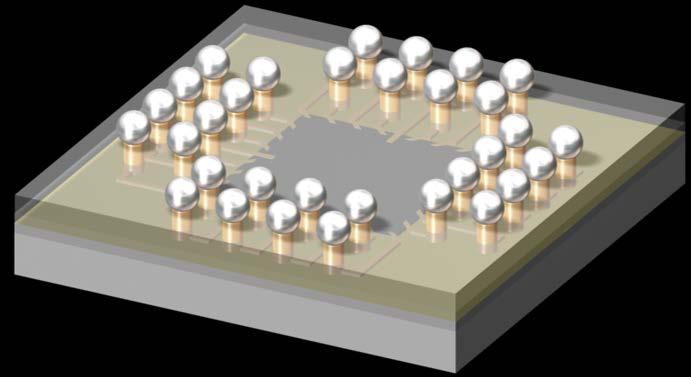
9 Package on Package (PoP) : traditional structures 9 Bottom Package: Flip chip die Bottom Package: Wire bonded die Standard size: 12x12mm


10 Advanced LGA SIP 10 Stacked & side-by-side configuration Diode SMDs

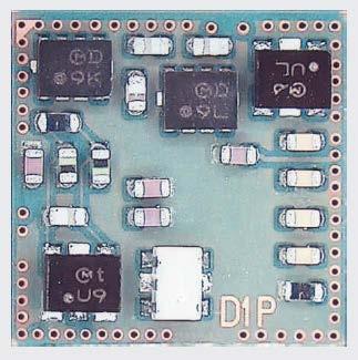
11 Embedded Die 11 Integration, miniaturization, shielding, short interconnections Embedded die
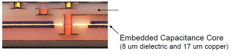

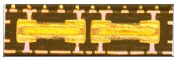
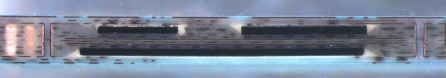
12 Embedded Capacitors 12 Embedded SMDs


13 From BGA WB to FC or FCCP BGA 13 Conventional Wire Bonded BGA Device Substrate Flip Chip with solder ball bumps Si Al Flip Chip with Copper Pillar bumps
 & micro bumps.")
14 What s 3D IC? 14 3D already exist at die or package level: wire bonding stacked dies. POP STACK POP 3D IC is related to interconnecting dies with high density and performance connections using TSV (Through Silicon Via) & micro bumps. µbumps Thin die Active face Logic die Wide-IO DRAM die TSV Bumps Substrate
 Type (via middle, via last ) Aspect ratio Electrical performances Thin wafer handling & processing Temporary carrier Compatibility with other")
15 3D IC Main Technology Enablers 15 Stacking Process Accuracy Underfill Type (Capillary, NCP ) Process Top die Bottom die Substrate Micro bumping Type (Cu pillar, CuCu ) Pitch Electrical performances Through silicon via (TSV) Type (via middle, via last ) Aspect ratio Electrical performances Thin wafer handling & processing Temporary carrier Compatibility with other process


16 die die wires Lead Frame Packages 16 leads full plastic exposed pad 1 layer metal frame with bent leads Reliability Thermal performance Cost but limited layout flexibility (only radial signals distribution)
17 Leads Shape Evolution 17 straight ( 70) J bent ( 80) gull wing ( 90) no leads! ( 00) DIP Power pack. PLCC, SOJ SO, TSOP, TSSOP, TQFP QFN, (BGA) pass through surface mount Methods to attach IC devices to PC board
18 Packaging Thickness Trend 18 Values in mm LQFP TQFP VQFPN U/W/VQFN-mr Resin /0.70/0.80 Die /0.140 Lead frame ~0.125 Standoff max max Total 1.60 max 1.20 max 1.00 max 0.65/0.8/1.0 max


19 QFNs Tapeless 19 Tapeless QFN QFN-mr (Quad Flatpack No lead Multi Row) QFN-sr (Quad Flatpack No lead Single Row)


20 QFN-mr: driving forces 20 L/TQFP exposed pad big dimensions thermal dissipation QFN-mr single row QFN pin count limited no leads BGA high cost & low power dissipation high pin count
21 QFN/QFN-mr: Package Characteristics 21 BGA cost & power dissipation e-tqfp dimensions & lead count QFN lead count QFN-mr package size (same I/O number) high pin count capability warpage excursion high frequency capability thermal dissipation MSL & SJR assembly (robust process) testing & finishing (robust process) TECHNOLOGY Multi row I/O Small footprint Free-routing cap. Single row I/O Large footprint Mature pck Single row I/O Small footprint Multi row I/O Smallest footprint Flexible I/O design worst best


22 Wafer Level Packaging 22 Fan In-WLP Fan Out-WLP (ewlb) Solder ball UBM (Under Bump Metallurgy) RDL (Al,Cu) Si Chip Solder ball Cu-RDL Si Chip EMC
23 Thank You! Packaging by ST
Semiconductor Manufacturing Technology. Semiconductor Manufacturing Technology
 Semiconductor Manufacturing Technology Michael Quirk & Julian Serda October 2001 by Prentice Hall Chapter 20 Assembly and Packaging Four Important Functions of IC Packaging 1. Protection from the environment
#$"&! "# % &(")# % %!!*,-
# % %!!*,-") ! "! #$% #$"&! '' "# % &(")# %!*+ %!!*,- . Flip Chip! Fine Pitch & Low-K Wire Bonding Test Program Conversion Substrate/Bumping/Assembly/Test Turnkey Solution! Stacked Die SIP BCC QFN MEMS Green Solutions!
! "! #$% #$"&! '' "# % &(")# %!*+ %!!*,- . Flip Chip! Fine Pitch & Low-K Wire Bonding Test Program Conversion Substrate/Bumping/Assembly/Test Turnkey Solution! Stacked Die SIP BCC QFN MEMS Green Solutions!
General Note #1 :Different kinds of IC Packages
 2012/09/01 09:08 1/9 General Note #1 :Different kinds of IC s General Note #1 :Different kinds of IC s Click to expand Image Name Description & Examples Ball Grid Array aka BGA BGA packages are used to
Advanced Topics. Packaging Power Distribution I/O. ECE 261 James Morizio 1
 Advanced Topics Packaging Power Distribution I/O ECE 261 James Morizio 1 Package functions Packages Electrical connection of signals and power from chip to board Little delay or distortion Mechanical connection
Cooling from Down Under Thermally Conductive Underfill
 Cooling from Down Under Thermally Conductive Underfill 7 th European Advanced Technology Workshop on Micropackaging and Thermal Management Paul W. Hough, Larry Wang 1, 2 February 2012 Presentation Outline
IME TSI Consortium Industry Forum
 Institute of Microelectronics IME TSI Consortium Industry Forum 2.5D Heterogeneous Integration on Through Silicon Interposers 17 th August 2012 1 IME Industry Forum on 2.5D Through Si Interposer (TSI)
 JAXA Microelectronics Workshop 23 National Aeronautics and Space Administration The Assurance Challenges of Advanced Packaging Technologies for Electronics Michael J. Sampson, NASA GSFC Co-Manager NASA
Underfilling Flip Chips on Hard Disk Drive Preamp Flex Circuits and SIPs on Substrates using Jetting Technology
 Underfilling Flip Chips on Hard Disk Drive Preamp Flex Circuits and SIPs on Substrates using Jetting Technology Michael Peterson Director, Advanced Engineering Belton mjpeterson@integraonline.com Steven
TRENDS IN AUTOMOTIVE SIP SYSTEMS: REVIEW BASED
 Electronic Costing & Technology Experts Power electronics MEMS & Sensors LED & Optoelectronics Advanced Packaging System TRENDS IN AUTOMOTIVE SIP SYSTEMS: REVIEW BASED ON TEARDOWN OF ACTUAL SOLUTIONS SiP
SURFACE MOUNT NOMENCLATURE AND PACKAGING
 SURFACE MOUNT NOMENCLATURE AND PACKAGING Tel 800-776-9888 Email info@topline.tv w w w. t o p l i n e. t v Contents Overview... 3 Flat Chip... 4 MELF Components...10 Tantalum Capacitors.... 12 Transistors
BOARD LEVEL RELIABILITY OF FINE PITCH FLIP CHIP BGA PACKAGES FOR AUTOMOTIVE APPLICATIONS
 As originally published in the SMTA Proceedings BOARD LEVEL RELIABILITY OF FINE PITCH FLIP CHIP BGA PACKAGES FOR AUTOMOTIVE APPLICATIONS Laurene Yip, Ace Ng Xilinx Inc. San Jose, CA, USA laurene.yip@xilinx.com
Library Expert Through-hole Families
 Non-polarized Axial Diameter Leaded Component Library Expert Through-hole Families Resistor (RESAD) Capacitor Non-polarized (CAPAD) Fuse Axial Diameter (FUSAD) Inductor Axial Diameter (INDAD) Non-polarized
IPC-7351B Electronic Component Zero Orientation For CAD Library Construction
 AppNote 10831 A P P N O T E S SM IPC-7351B Electronic Zero Orientation For CAD Library Construction Copyright 2010 Mentor Graphics Corporation Trademarks that appear in Mentor Graphics product publications
Motor Driver PCB Layout Guidelines. Application Note
 AN124 Motor Driver PCB Layout Guidelines Motor Driver PCB Layout Guidelines Application Note Prepared by Pete Millett August 2017 ABSTRACT Motor driver ICs are able to deliver large amounts of current
Getting the Lead Out December, 2007
 Getting the Lead Out December, 2007 Tom DeBonis Assembly & Test Technology Development Technology and Manufacturing Group Summary Intel has removed the lead (Pb) from its manufacturing process across its
A Trace-Embedded Coreless Substrate Technique
 A Trace-Embedded Coreless Substrate Technique Chang-Yi(Albert) Lan, 藍章益 SPIL (Siliconware Precision Industries Co., Ltd) No. 153, Sec. 3, Chung Shan Rd, Tantzu Dist, Taichung, Taiwan, R.O.C. Outline Introduction
PLCC Plastic Leaded Chip Carrier
 PLCC Plastic ed Chip Carrier Plastic ed Chip Carriers (PLCC) are four-sided J ed Plastic body packages. counts range from 20 to 84. PLCC packages can be square or rectangle. Body sizes range from.35" to
7331A Garden Grove Blvd, Garden Grove, CA Tel Fax
 (R) 7331A Garden Grove Blvd, Garden Grove, CA 92841 Tel. 1-800-776-9888 Fax 1-714-891-0321 e-mail info@topline.tv www.topline.tv c 1998 TopLine. All Rights Reserved Table of Contents Definition of Dummy
GT Silver Button Technology Socket for Semiconductor Test
 GT Silver Button Technology Socket for Semiconductor Test Toll Free: (800) 404-0204 U.S. Only Tel: (952) 229-8200 Fax: (952) 229-8201 email: info@ironwoodelectronics.com Application Need Prototype Test
SURFACE MOUNT ASSEMBLY AND BOARD LEVEL RELIABILITY FOR HIGH DENSITY POP (PACKAGE-ON-PACKAGE) UTILIZING THROUGH MOLD VIA INTERCONNECT TECHNOLOGY
 UTILIZING THROUGH MOLD VIA INTERCONNECT TECHNOLOGY") SURFACE MOUNT ASSEMBLY AND BOARD LEVEL RELIABILITY FOR HIGH DENSITY POP (PACKAGE-ON-PACKAGE) UTILIZING THROUGH MOLD VIA INTERCONNECT TECHNOLOGY Curtis Zwenger, Lee Smith, and *Jeff Newbrough Amkor Technology
SURFACE MOUNT ASSEMBLY AND BOARD LEVEL RELIABILITY FOR HIGH DENSITY POP (PACKAGE-ON-PACKAGE) UTILIZING THROUGH MOLD VIA INTERCONNECT TECHNOLOGY Curtis Zwenger, Lee Smith, and *Jeff Newbrough Amkor Technology
SMD PACKAGES. Contents. 3. Packages with four or more terminals
 MANTECH ELECTRONICS Internatinal Cmpnents Distributr TEL JHB : (011) 493-9307 CAPE : (021) 535-3150 KZN : (031) 309-7692 FAX : (011) 493-9319 sales@mantech.c.za www.mantech.c.za SMD PACKAGES Cntents 1.
Designing for Cost Effective Flip Chip Technology
 Designing for Cost Effective Flip Chip Technology Jack Bogdanski White Electronic Designs Corp. Designing For Cost Effective Flip Chip Technology Bump and fl ip approaches to semiconductor packaging have
Devices and their Packaging Technology
 4 th Workshop Future of Electronic Power Processing and Conversion Devices and their Packaging Technology May 2001 Werner Tursky SEMIKRON ELEKTRONIK GmbH Nuremberg, Germany 1 1. Devices 2. From Discrete
Core Power Delivery Network Analysis of Core and Coreless Substrates in a Multilayer Organic Buildup Package
 Core Power Delivery Network Analysis of Core and Coreless Substrates in a Multilayer Organic Buildup Package Ozgur Misman, Mike DeVita, Nozad Karim, Amkor Technology, AZ, USA 1900 S. Price Rd, Chandler,
PACKAGE INFORMATION 5. THERMAL-RESISTANCE OF IC PACKAGE
 This version: Apr. 2001 Previous version:jun. 1997 PACKAGE INFORMATION 5. THERMAL-RESISTANCE OF IC PACKAGE This document is Chapter 5 of the package information document consisting of 8 chapters in total.
Package Outline Diagram Page Layout Used in This Data Book
 Package Outline Diagram Page Layout Used in This Data Book Header: Shows form and number of pins FINE PITCH BALL GRID ARRAY PACKAGE 176 PIN PLASTIC Package code BGA-176P-M03 176-pin plastic FBGA Lead pitch
Jet Dispensing Underfills for Stacked Die Applications
 Jet Dispensing Underfills for Stacked Die Applications Steven J. Adamson Semiconductor Packaging and Assembly Product Manager Asymtek Sadamson@asymtek.com Abstract It is not uncommon to see three to five
Hitachi Semiconductor Package Data Book
 Hitachi Semiconductor Package Data Book ADE-410-001K 12th Edition September/2002 Semiconductor & Integrated Circuits Hitachi, Ltd. Introduction Thank you for using Hitachi s semiconductor devices. The
Thermal Characterization and Modeling: a key part of the total packaging solution. Dr. Roger Emigh STATS ChipPAC Tempe, AZ
 Thermal Characterization and Modeling: a key part of the total packaging solution Dr. Roger Emigh STATS ChipPAC Tempe, AZ Outline: Introduction Semiconductor Package Thermal Behavior Heat Flow Path Stacked
engineered to connect Full Product Line
 engineered to connect Full Product Line TEST solutions The technical data and specifications of the products shown in this catalogue are for reference only, and apply to products available at the time
About Us. even in allocation times.
 History The company SIEGERT was founded in 1945 by Dipl.-Ing. Ludwig Siegert. During the 50ies the enterprise focused on the manufacturing of film resistors. 1965 was the start of production of miniaturized
Flat Packages Mounting Adhesives
 Flat Packages Mounting Adhesives Introduction Both consumers and industry are demanding that electronic equipment integrated with IC or LSI be made smaller and lighter, and have enhanced features. Products
Automotive Technology
 Automotive Technology Advanced Technology for Automotive Applications Design, Manufacture & Test www.cmac.com C-MAC MicroTechnology is a leader in the manufacture and test of complex, high-reliability
Realization of a New Concept for Power Chip Embedding
 As originally published in the SMTA Proceedings Realization of a New Concept for Power Chip Embedding H. Stahr 1, M. Morianz 1, I. Salkovic 1 1: AT&S AG, Leoben, Austria Abstract: Embedded components technology
Evolving Bump Chip Carrier
 FUJITSU INTEGRATED MICROTECHNOLOGY LIMITED. The Bump Chip Carrier, which was developed as a small pin type, miniature, and lightweight CSP, is not only extremely small due to its characteristic structure,
Embedding Energy Storage in SoCs using Solid State Batteries. PowerSoC 12 November 16, 2012
 Embedding Energy Storage in SoCs using Solid State Batteries PowerSoC 12 November 16, 2012 Key Trends Driving Innovation Ultra Low Power Processors Smart Devices and Sensors Everywhere Wireless is pervasive
Product Information. Allegro Package Designations
 Product Information Allegro Designations This document provides reference information as an aid to differentiating the device package types used by Allegro MicroSystems. It provides cross-references to
Eutectic Sn/Pb Fine-Pitch Solder Bumping and Assembly for Rad-Hard Pixel Detectors
 Eutectic Sn/Pb Fine-Pitch Solder Bumping and Assembly for Rad-Hard Pixel Detectors Alan Huffman MCNC Advanced Packaging and Interconnect Sept 11, 2002 Outline MCNC Overview Solder Bumping Overview Fermilab
MAXIMUM. Mill-Max Introduces Gull Wing SMT.070 Pitch ShrinkDIP & SIP Sockets and Headers
 MAXIMUM solutions Mill-Max Introduces Gull Wing SMT.070 Pitch ShrinkDIP & SIP Sockets and Headers Mill-Max series 117, 127, 217 & 227 shrinkdip sockets accommodate memory chips and components which have
Scorpion. Rework System
 Scorpion Rework System MEET THE SCORPION REWORK SYSTEM The Scorpion Advanced Package Rework System ensures both accurate component placement and custom tailored reflow profiles in one user friendly, single
Preface. Fujitsu Limited
 Preface Thank you for your continuing loyalty to Fujitsu's semiconductor products. Electronic equipment is continually becoming smaller, lighter, and less expensive while also growing more advanced in
300mm Wafer Electroless Bumping
 300mm Wafer Electroless Bumping T. Teutsch, E. Zakel, T. Oppert Internepcon 2005 January 19, 2005 Tokyo Big Sight, Japan Pac Tech GmbH Outline Short Company Profile Introduction Electroless Ni/Au Under
Coreless Packaging Technology for High-performance Application
 62 nd ECTC San Diego, CA: May 29 June 1, 2012 Coreless Packaging Technology for High-performance Application Corp Advanced LSI Assembly Product Department Analog LSI Bussiness Division Semiconductor Business
Schedule. VLSI Design : Package 1
 Schedule 03. 09/27/18 Chapter 5 (Memory devices: RAM, Clock skew) 04. 10/04/18 Chapter 5 (Memory timing and clock, Testing) 05. 10/11/18 Chapter 5 (Sequential machine, State graph) 06. 10/18/18 (QZ1) Packaging
Table of Contents PLCC QFP/MQFP/FQFP/CQFP LQFP/TQFP PQFP BQFP LCC/LCCC DFN QFN...61 QFN Multiple Row...
 Table of Contents Terminology Introduction... 2 Through Hole vs. Surface Mount.... 3 Through Hole Leads...3, 4 Surface Mount Leadless... 4 Surface Mount Leaded.... 5 Component Packaging...6 Identifying
Fine Pitch Cu Pillar with Bond on Lead (BOL) Assembly Challenges for High Performance Flip Chip Package
 Assembly Challenges for High Performance Flip Chip Package") Fine Pitch Cu Pillar with Bond on Lead (BOL) Assembly Challenges for High Performance Flip Chip Package by Nokibul Islam, Vinayak Pandey, *KyungOe Kim STATS ChipPAC Inc Fremont, CA, USA *STATS ChipPAC
Fine Pitch Cu Pillar with Bond on Lead (BOL) Assembly Challenges for High Performance Flip Chip Package by Nokibul Islam, Vinayak Pandey, *KyungOe Kim STATS ChipPAC Inc Fremont, CA, USA *STATS ChipPAC
Surface MEMS Design Examples Dr. Lynn Fuller Webpage:
 ROCHESTER INSTITUTE OF TECHNOLOGY MICROELECTRONIC ENGINEERING Surface MEMS Design Examples Webpage: http://people.rit.edu/lffeee 82 Lomb Memorial Drive Rochester, NY 14623-5604 Tel (585) 475-2035 Email:
1. Fundamentals of microsystems packaging
 1. Fundamentals of microsystems packaging 1.1 Introduction A microsystem is a miniaturized electronic system that combines micro-passive structures, micro-sensors, micro-actuators and micro-processing
System. Specifications
 Kit Part Numbering System WebCode XK1 926 Series 900 = QFP Lead Template 901 = FC176 Flip Chip 902 = FC88 Flip Chip 903 = FC317 Flip Chip 904 = FC220 Flip Chip 905 = CBGA Ceramic Substrates 906 = FC96
June 13, 2012 Presentation for CTEA Symposium
 TM June 13, 2012 Presentation for CTEA Symposium Freescale, the Freescale logo, AltiVec, C-5, CodeTEST, CodeWarrior, ColdFire, C-Ware, the Energy Efficient Solutions logo, mobilegt, PowerQUICC, QorIQ,
Support Products & Consumables
 Support Products & Consumables Solder, Desolder & Rework SMT & Area Array Rework Fume Extraction Solutions and systems for soldering, rework and repair of electronics worldwide Table of Contents Systems
TND6031/D. Introducing Intelligent Power Module (IPM) Family from ON Semiconductor TECHNICAL NOTE THE TECHNOLOGY
 Family from ON Semiconductor TECHNICAL NOTE THE TECHNOLOGY") Introducing Intelligent Power Module (IPM) Family from ON Semiconductor TECHNICAL NOTE THE TECHNOLOGY Insulated Metal Substrate Technology (IMST ) ON Semiconductor became the first company in the world
Introducing Intelligent Power Module (IPM) Family from ON Semiconductor TECHNICAL NOTE THE TECHNOLOGY Insulated Metal Substrate Technology (IMST ) ON Semiconductor became the first company in the world
gan power Energy-efficient power electronics with Gallium Nitride transistors Leti, technology research institute Contact:
 gan power Energy-efficient power electronics with Gallium Nitride transistors, technology research institute Contact: leti.contact@cea.fr A market in growth GaN devices for next-era power-electronics applications
Versatile Z-Axis Interconnection-Based Coreless Technology Solutions for Next Generation Packaging
 Versatile Z-Axis Interconnection-Based Coreless Technology Solutions for Next Generation Packaging R.N. Das, F.D. Egitto, J. M. Lauffer, Evan Chenelly and M. D. Polliks Endicott Interconnect Technologies,
Application of fccube TM Technology to Enable Next Generation Consumer Device
 Application of fccube TM Technology to Enable Next Generation Consumer Device by Simon Stacey**, Jonathan Wei** **CSR Nokibul Islam*, Mukul Joshi*, Cory Lindholm*, KeonTaek Kang*, JoungIn Yang*, Gwang
Contacting various metal compositions using ViProbe Vertical Technology
 Denis Deegan Analog Devices Inc Simon Allgaier Feinmetall GmbH Contacting various metal compositions using ViProbe Vertical Technology June 6 to 9, 2010 San Diego, CA USA Content Motivation. ViProbe Vertical
F.O.B. ex-works TopLine USA. Please specify preferred method of shipment when placing order.
 2018 Kits HOW TO ORDER Payment Terms Credit Terms (Net 30) for established customers. American Express, Mastercard and VISA accepted. Confirming Purchase Orders Confirming purchase orders are required
3M Textool Test and Burn-In Sockets for 1.0 mm Area Array Packages Including Ball Grid Array and Land Grid Array
 3M Textool Test and Burn-In Sockets for 1.0 mm Area Array Packages Including Ball Grid Array and Land Grid Array 1.0 mm Pitch Socket Platforms Socket Max. Package Maximum Max. Pin Lid Series Product Number
gan power Energy-efficient Power Electronics using Gallium Nitride Transistors Leti, technology research institute Contact:
 gan power Energy-efficient Power Electronics using Gallium Nitride Transistors, technology research institute Contact: leti.contact@cea.fr A GROWTH MARKET GaN Devices for Next-Era Power Electronics $ 600.0M
Cooling Assessment and Distribution of Heat Dissipation of A Cavity Down Plastic Ball Grid Array Package - NuBGA
 Cooling Assessment and Distribution of Heat Dissipation of A Cavity Down Plastic Ball Grid Array Package - NuBGA Cooling Assessment and Distribution of Heat Dissipation of A Cavity Down Plastic Ball Grid
EV/HEV Automotive Power Modules: Innovations and trends
 EV/HEV Automotive Power Modules: Innovations and trends Elena Barbarini, Phd IMAPS 2018, 8th November 22 Bd Benoni Goullin 44200 NANTES - FRANCE +33 2 40 18 09 16 info@systemplus.fr www.systemplus.fr 2018
MS52XX SMD Pressure Sensor
 1, and 12 bar absolute pressure range Uncompensated Piezoresistive silicon micromachined sensor Surface mount 7.6 x 7.6 mm Low-noise, high-sensitivity, high-linearity DESCRIPTION The MS52XX SMD pressure
Towards a PowerSoC Solution for Automotive Microcontroller Applications
 Towards a PowerSoC Solution for Automotive Microcontroller Applications Christoph Sandner, Gerhard Maderbacher, Karlheinz Kogler, Joachim Pichler, Federico Capponi, Herbert Gruber, Sylvia Michaelis, Dietrich
Future Challenges in BGA/CSP Rework Patrick McCall PACE Incorporated Laurel, Maryland, USA
 Future Challenges in BGA/CSP Rework Patrick McCall PACE Incorporated Laurel, Maryland, USA Introduction: Over the last 2 to 3 years, standard area array packages have become the package of choice in both
Temperature Cycling of Coreless Ball Grid Arrays
 Temperature Cycling of Coreless Ball Grid Arrays Daniel Cavasin, Nathan Blattau, Gilad Sharon, Stephani Gulbrandsen, and Craig Hillman DfR Solutions, MD, USA AMD, TX, USA Abstract There are countless challenges
Tape and Reel Packaging
 Tape and Reel Packaging Introduction The electronics industry is making a tremendous investment in surfacemount technology. The reasons for this investment include cost savings resulting from automated
The MiCS-2714 is a compact MOS sensor.
 Rs/R0 Data Sheet The is a compact MOS sensor. The is a robust MEMS sensor for nitrogen dioxide and leakage detection. Features Smallest footprint for compact designs (5 x 7 x 1.55 mm) Robust MEMS sensor
White Paper: Pervasive Power: Integrated Energy Storage for POL Delivery
 Pervasive Power: Integrated Energy Storage for POL Delivery Pervasive Power Overview This paper introduces several new concepts for micro-power electronic system design. These concepts are based on the
Support Products & Consumables
 Support Products & Consumables Solder, Desolder & Rework SMT & Area Array Rework Fume Extraction Solutions and systems for soldering, rework and repair of electronics Table of Contents Systems ST Systems
Copper Clip Package for high performance MOSFETs and its optimization
 Copper Clip Package for high performance MOSFETs and its optimization Kyaw Ko Lwin, Carolyn Epino Tubillo, Panumard T., Jun Dimaano, Dr. Nathapong Suthiwongsunthorn, Saravuth Sirinorakul United Test and
Ultra-Small Absolute Pressure Sensor Using WLP
 Ultra-Small Absolute Pressure Sensor Using WLP Shinichi Murashige, 1 Satoshi Yamamoto, 2 Takeshi Shiojiri, 2 Shogo Mitani, 2 Takanao Suzuki, 3 and Mikio Hashimoto 4 Recently, as the miniaturization and
Inverter Market Trends and Major Technology Changes
 Inverter Market Trends 2013-2020 and Major Technology Changes February 2013 A big dive into the heart of the power electronics industry, from systems to active & passive components REPORT SAMPLE Delphi
EP A2 (19) (11) EP A2 (12) EUROPEAN PATENT APPLICATION. (43) Date of publication: Bulletin 2007/47
 (11) EP A2 (12) EUROPEAN PATENT APPLICATION. (43) Date of publication: Bulletin 2007/47") (19) (12) EUROPEAN PATENT APPLICATION (11) EP 1 88 077 A2 (43) Date of publication: 21.11.2007 Bulletin 2007/47 (1) Int Cl.: H01L 23/367 (2006.01) H01L 2/06 (2006.01) (21) Application number: 070731.2
(19) (12) EUROPEAN PATENT APPLICATION (11) EP 1 88 077 A2 (43) Date of publication: 21.11.2007 Bulletin 2007/47 (1) Int Cl.: H01L 23/367 (2006.01) H01L 2/06 (2006.01) (21) Application number: 070731.2
Mitsubishi Electric Semi-Conductors Division. IGBT Module 7th Generation T-Series. June 14, 2018
 Mitsubishi Electric Semi-Conductors Division IGBT Module 7th Generation T-Series June 14, 2018 7 th generation IGBT module SLC-Technology (SoLid Cover Technology) Optimized structure with resin insulation
680 Series QFP Socket
 0805 680 QFP Socket Open top, Zero Insertion Force design for automatic loading Compact outline for maximum board density Highly reliable Dual Beam contact design, "H" version Lid actuation force peaks
28nm CPI (Chip/Package Interactions) in Large Size ewlb (Embedded Wafer Level BGA) Fan-Out Wafer Level Packages
 in Large Size ewlb (Embedded Wafer Level BGA) Fan-Out Wafer Level Packages") 28nm CPI (Chip/Package Interactions) in Large Size ewlb (Embedded Wafer Level BGA) Fan-Out Wafer Level Packages by Kang Chen, Linda Chua, Won Kyung Choi, Seng Guan Chow and Seung Wook Yoon* STATS ChipPAC
28nm CPI (Chip/Package Interactions) in Large Size ewlb (Embedded Wafer Level BGA) Fan-Out Wafer Level Packages by Kang Chen, Linda Chua, Won Kyung Choi, Seng Guan Chow and Seung Wook Yoon* STATS ChipPAC
IRDA-WELDER User Manual Model: TX-999DM
 IRDA-WELDER User Manual Model: TX-999DM DRAGON GROUP CHINA INTERNATIONAL PUHUIT BGA DESK DEVICES DIVISION http://www.puhuit.com CONTENT 1. Features 2 2. Main Parameter 3 3. Main Components 4 4. Description
SUPPORT PRODUCTS AND CONSUMABLES SOLUTIONS FOR THE ELECTRONICS INTERCONNECTION PROCESS
 GSA Service Company Military/Gov't Manufacturer's Representative 1310 E. Maple Ave Sterling, VA 20164 703-731-8048 www.gsaservice.com SUPPORT PRODUCTS AND CONSUMABLES SOLUTIONS FOR THE ELECTRONICS INTERCONNECTION
Power Supplies Advanced Materials for Higher Performance. Tech Taipei 2017 Sep 21, 2017
 Power Supplies Advanced Materials for Higher Performance Tech Taipei 2017 Sep 21, 2017 Agenda 1. Henkel Company Introduction 2. Power Technology Trend 3. Application & Solution Overview - Transistors to
Electronic materials and components-a component review
 Electronic materials and components-a component review Through-hole components We start our review of components by looking at those designs with leads that are intended to be soldered into through-holes
Product Range BGA Rework Stations
 Product Range BGA Rework Stations PDR IR-E6 Evolution XL Ultimate Performance, BGA Rework System for Very Large PCBs Medium - large sized PCBs - SMDs, BGAs, ubgas Software controlled, Focused IR process
Building Blocks and Opportunities for Power Electronics Integration
 Building Blocks and Opportunities for Power Electronics Integration Ralph S. Taylor APEC 2011 March 8, 2011 What's Driving Automotive Power Electronics? Across the globe, vehicle manufacturers are committing
74x Series Chip Resistor Arrays
 Features Low Cost Thick Film Technology Leadless Surface Mount Construction Concave Convex Terminations Solder Coated Nickel Barrier Pads Isolated and Bussed Circuit Configurations Improved TCR Tracking
Process Considerations when Reworking Area Array Packages Patrick McCall PACE Incorporated Laurel, Maryland, USA
 Process Considerations when Reworking Area Array Packages Patrick McCall PACE Incorporated Laurel, Maryland, USA Introduction: Over the last 2 to 3 years, standard area array packages have become the package
Low TCR, 1mW Dual Rejustor Micro-Resistor MBD-472-AL
 Low TCR, 1mW Dual Rejustor Micro-Resistor MBD-472-AL The Rejustor is a precision, electrically-adjustable resistor from Microbridge. The Rejustor can be adjusted to a precision of 0.1%, or better. The
TEMPERATURE SENSORS TEMPERATURE SENSORS
 TEMPERATURE SENSORS TE Connectivity is a leader in the design and manufacture of NTC thermistors, RTDs, thermocouples, thermopiles, digital output and customized sensor assemblies. Building on our long
HADES Workshop. May 24-26, 2011 Perma Works LLC. My thanks to the GNS and Tiger Energy Services. Randy Normann, CTO
 HADES Workshop May 24-26, 2011 Perma Works LLC My thanks to the GNS and Tiger Energy Services Randy Normann, CTO randy@permaworks.com Perma Works LLC Albuquerque, New Mexico, USA Perma Works Acquiring
IGBT5 and. The new Chip Generation and its innovative Interconnection Technology. PCIM 2014, Nuremberg
 IGBT5 and The new Chip Generation and its innovative Interconnection Technology, Nuremberg IGBT5 and.xt Technology offers Key Features Useable operation temperature up to Tvjop=175 C Optimized switching
Index. bulk micromachining 2 3, 56, 94 96, 109, 193, 248
 Index ablation 82, 84 accelerometer manufacturers 197, 220 accelerometers 2 4, 7, 9, 126 27, 168 69, 179, 197, 200 1, 204, 210, 212 14, 216 20, 239 41, 249 51, 279 80 digital 200 single-axis 197 98 single-die
New Reliability Assessment Methods for MEMS. Prof. Mervi Paulasto-Kröckel Electronics Integration and Reliability
 New Reliability Assessment Methods for MEMS Prof. Mervi Paulasto-Kröckel Electronics Integration and Reliability Aalto University A merger of leading Finnish universities in 2010: Helsinki School of Economics
All-SiC Module for Mega-Solar Power Conditioner
 All-SiC Module for Mega-Solar Power Conditioner NASHIDA, Norihiro * NAKAMURA, Hideyo * IWAMOTO, Susumu A B S T R A C T An all-sic module for mega-solar power conditioners has been developed. The structure
High-Speed Piezoelectric Jet Valves Offer New Modular Dispensing Solutions
 High-Speed Piezoelectric Jet Valves Offer New Modular Dispensing Solutions Published by: Nordson EFD, 40 Catamore Boulevard, East Providence, RI 02904 2013 Nordson Corporation www.nordsonefd.com Table
Preface. Fujitsu Limited Electronic Devices
 Preface Thank you for your continuing loyalty to Fujitsu's semiconductor products. Electronic equipment is continually becoming smaller, lighter, and less expensive while also growing more advanced in
Trends and Considerations in Automotive Electronic Packaging
 PACKAGING Trends and Considerations in Automotive Electronic Packaging Deborah Patterson, Marc Mangrum, Adrian Arcedera, John Sniegowski Amkor Technology Automotive Electronic Content Growth The transition
The Connector. Bob Willis OHIO VALLEY OFFICERS. Ohio Valley Chapter
 Dec. 9th, 2011 FRIDAY 9:00 A.M. to 3:30 P.M. SMTA Members/Non Members $35/$55 Student members/non-members $5/$10 Lunch Included. Cash or Check at the Door RSVP ASAP (by Dec. 5th, 2011) to Ohio Valley Chapter
MultiGig RT Product Family Slot Pitch Density Data Rate RT lines/inch Gbps lines/inch Gbps RT lines/inch 6.50 Gbp
 1 MultiGig RT Assembly! # # "$#! MultiGig RT Product Family Slot Pitch Density Data Rate RT1 0.8 113 lines/inch 3.125 Gbps 1.0 141 lines/inch 3.125 Gbps RT2 0.8 85 lines/inch 6.50 Gbps* 1.0 113 lines/inch
NP276 Series (Open Top)
") Ball Grid Array (BGA, 1.27mm Pitch) Specifications Insulation Resistance: Dielectric Withstanding Voltage: Contact Resistance: Operating Temperature Range: Contact Force: Mating Cycles: Materials and Finish
Ball Grid Array (BGA, 1.27mm Pitch) Specifications Insulation Resistance: Dielectric Withstanding Voltage: Contact Resistance: Operating Temperature Range: Contact Force: Mating Cycles: Materials and Finish
AEC-Q100G Qualification Results
 Objective: MCU5643LFF2MLQ1 (Leopard) ATMC Cu Wire Qualification On 144LQFP Freescale PN: MCU5643LFF2MLQ1 Customer Name(s): "Varies" Part Name: Leopard PN(s): "Varies" Technology: CMOS90FG Package: LQFP
NASA-DoD Lead-Free Electronics Project
 NASA-DoD Lead-Free Electronics Project June 24, 2009 Tin Whisker Group Telecon Slide 1 Testing project will build on the results from the JCAA/JGPP LFS Project The primary technical objective of this project
ELECTRONICS. Power Distribution Technology
 ELECTRONICS Power Distribution Technology with 14,000 employees in 30 countries and sales of 1.1 1.28 billion billion euros euros in 2011, in 2010 FCI is a global manufacturer of connectors for various