Schedule. VLSI Design : Package 1
|
|
|
- Jared Wheeler
- 5 years ago
- Views:
Transcription
1 Schedule /27/18 Chapter 5 (Memory devices: RAM, Clock skew) /04/18 Chapter 5 (Memory timing and clock, Testing) /11/18 Chapter 5 (Sequential machine, State graph) /18/18 (QZ1) Packaging (Flow) /25/18 Packaging (Reliability) /01/18 Midterm Examination 校慶 VLSI Design : Package 1
2 Packaging Functional: Signal and Power connections Make possible for the next level connections Provide adequate protection (mechanical and environmental) Electrical: Low parasitic Thermal Removal: Efficient heat removal Mechanical: Reliable and robust Economical: Cheap (material and manufacture throughput) VLSI Design : Package 2
3 Materials Metal -- Signal connection -- Heat conductivity Ceramic -- Expensive -- Physical characteristics Plastic -- Cheap -- Physical characteristics (heat ) VLSI Design : Package 3
4 Packaging Flow Wafer => Wafer Probe (WP) => Dicing => Bonding => Packaged Design Layout Masks Photolithographic Package Wafer Process Chips => Burn-in, Final Test (FT) VLSI Design : Package 4
 Lead Frame Chip")

5 Appearance ( DIE ) Lead Frame Chip Lead Frame VLSI Design : Package 5
6 Design Layout Masks Photolithographic Package Wafer Process Bonding Chips Wire Bonding Wire Substrate Die Pad Lead Frame VLSI Design : Package 6
7 TAB (Tape-Automated Bonding) Sprocket hole Film + Pattern Solder Bump Test pads Die Lead frame Substrate (b) Die attachment using solder bumps. (a) Polymer Tape with imprinted wiring pattern. Polymer film VLSI Design : Package 7


8 VLSI Design : Package 8
9 Requirement for Qualification Testing Items Conditions Criteria (Target) =================================================================================== High Temp. Operating Life 125 deg.c /V CC abs max hr Low Temp. Operating Life -40 deg.c /V CC abs max hr High Temp. Storage 150 deg.c hr Low Temp. Storage -65 deg.c [*3] hr Temp. Humidity with Bias [*1] 85 deg.c /85 %RH /V CC hr HAST [*1] 130 deg.c /85 %RH hr hr ) Temp. Cycling [*1] -65/150 deg.c r=0@100 cy (r=0@1,000 cy ) Heat Shock [*1] -65/150 deg.c r=0@15cy (r=0@100 cy ) Solderability 245 deg.c /5 sec more than 95 % soldering ESD Immunity HBM +/-2,000 V MM +/-200 V CDM +/-1,000 V as JEITA (+/-1,500 V ) Corner:+/-750 V, Other:+/-500 V as ESDA Latch-up Immunity PCIM +/-125 ma as JEITA&JEDEC [*4] (+/-150 ma ) PSOV V CC abs max. as JEITA&JEDEC Package Immunity [*2] No delamination & no cracking [*5] =================================================================================== [*1] Pre-conditioning : for SMD : Bake(125 deg.c /24 hr ) Soak(30 deg.c /70 %RH /240 hr ) Re-flow [*2] for THD : Soldering heat (260deg.C/10sec), immersed to stopper [*2] Re-flow profile : according to JEDEC profile, SMD only [*3] Renesas condition : -40 deg.c [*4] Renesas criterion : +/-100 ma [*5] Refer to next page VLSI Design : Package 9

10 Criteria for Package Immunity <<Top View>> <<Cross-section View>> Outer lead Inner lead Chip Wire Molding VLSI Design : Package 10 Acceptable delamination area
11 Cross-section Wafer backside grinding die Gold / Copper Wire Lead Frame Silver Epoxy Die Pad Coating: 10% Pb, 90% Ti Buffer for different thermal expansion coefficients VLSI Design : Package 11
12 Thermal Dissipation 15 ~ 20 % (with heat sink 40 ~ 75%) 5 ~ 10 % (about the same) 70 ~ 80 % (25 ~ 50%) VLSI Design : Package 12


13 Design Layout Masks Photolithographic Package Wafer Process Package and Heat Chips Package types: Plastic: Below 1 watt Ceramic: Below 5 watt Special: Up to 30 watt VLSI Design : Package 13
14 CIP / SIP 30 mil Min. 12mil Max 12 mil Min. PKG Thickness (Min): 2.05mm 80mil DIE 2 : 10mil DIE 1 : 10 mil 8 mil Min. L/F thickness : 0.15mm 6mil BLT 1 0.2~1.4 mil BLT 2 (1~2 mil) Might be different processes VLSI Design : Package 14
 dies The")

15 MCM (Multi-Chip Module) dies The module failed, if any die failed VLSI Design : Package 15
16 MCM Size and weight Better performance: Decrease loading of external signals Reduce packaging cost of individual chips Yield Problem: (will increase the cost) If Single chip faults: 5% MCM yield with 10 chips: (0.95) 10 = 60% Heat density problem VLSI Design : Package 16

17 Design Layout Masks Photolithographic Package Wafer Process Flip Chip Chips Die Solder bumps Interconnect layers Substrate VLSI Design : Package 17


18 COF D CL I A C E CL F G VLSI Design : Package 18


19 Soft PCB 穿戴式系統 VLSI Design : Package 19


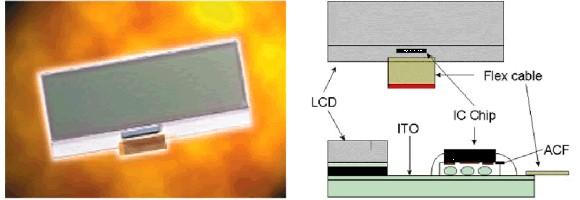
20 COG VLSI Design : Package 20


21 Wafer Level Packaging VLSI Design : Package 21

22 WLP Dallas Semiconductor Wafer Level Package VLSI Design : Package 22


23 What is a 3D IC? Could be Heterogeneous Stacked 2D (Conventional) ICs VLSI Design : Package 23

24 VLSI Design : Package 24

25 Prepackaging Flow I VLSI Design : Package 25


26 Prepackaging (1) 於 wafer 正面貼上研磨膠紙避免刮傷或污染 研磨 wafer 被面 VLSI Design : Package 26


27 Prepackaging (2) 撕下 wafer 正面研磨膠紙避免留下任何殘留 於 wafer 被面貼上切割膠紙以避免切割時晶粒飛濺 VLSI Design : Package 27


28 Prepackaging (3) 於 wafer 正面切割 wafer 切割膠紙並未切斷 照射 UV 軟化切割膠紙的黏性 VLSI Design : Package 28

29 Prepackaging Flow II VLSI Design : Package 29


30 Prepackaging (3) VLSI Design : Package 30


31 Glue Requirements Thickness: > 0.2mils 80% on each side and < 0.2mm Overflow < 2/3 of the die thickness Tilt < 2 mils Bubble area < 15% VLSI Design : Package 31

32 Example VLSI Design : Package 32


33 Die Cracking VLSI Design : Package 33
34 Reliability Different applications * Medical parts * Transportation components * 3C parts * Gifts, toys Testing items * function, timing * Thermal shock, shipping, vibration, humidity, chemical * Over Life time, burn-in VLSI Design : Package 34

35 Prepackaging- Bonding VLSI Design : Package 35

36 Gold Wire VLSI Design : Package 36


37 VLSI Design : Package 37

38 晶片邊緣與晶片座的間距 VLSI Design : Package 38
39 內部鋁墊與晶體邊緣的距離 為避免金線與晶體邊緣短路, 最長線長應被考慮, 且與模流方向有關係 VLSI Design : Package 39

40 銲墊設計 VLSI Design : Package 40


41 金線弧高設定 有接地線 交錯鋁墊 VLSI Design : Package 41
42 Schedule /27/18 Chapter 5 (Memory devices: RAM, Clock skew) /04/18 Chapter 5 (Memory timing and clock, Testing) /11/18 Chapter 5 (Sequential machine, State graph) /18/18 (QZ1) Packaging (Flow) /25/18 Packaging (Reliability) /01/18 Midterm Examination 校慶 VLSI Design : Package 42
43 Midterm Examination Next Week!! 35% Please Bring Your Photo ID!! Covered Chapter 5 to Today s material Seats will be rearranged VLSI Design : Package 43

44 VLSI Design : Package 44
45 銲墊設計 VLSI Design : Package 45

46 VLSI Design : Package 46
 VLSI Design :")
47 Inner Lead Short CWT QFP64(14*14) VLSI Design : Package 47


48 Lead Frame Tape VLSI Design : Package 48

49 Lead Frame Tape VLSI Design : Package 49


50 耗材 金線 99.99% Holding Clamps 熱壓版 Capillary 針頭 VLSI Design : Package 50

51 阻抗 VLSI Design : Package 51

52 Bonding Analysis VLSI Design : Package 52


53 Defects VLSI Design : Package 53

54 Defects VLSI Design : Package 54

55 Defects (Flip Chip) VLSI Design : Package 55

56 Post-packaging - Molding 175 degree C preheat VLSI Design : Package 56

57 Dejunk and Trimming Dam Bar Dejunk VLSI Design : Package 57

58 Forming VLSI Design : Package 58
59 Mark / Labling Ink Mark: Delivered the information including manufacture, product type, design team, revision, date, area, tracking code, or special codes Laser Mark: Used in tiny packages or for the environmental protection VLSI Design : Package 59

60 Pitch Center 2 center VLSI Design : Package 60
61 Bonding Options Wire Bonding: ~ 1000 connections TAB: 10 ~ couple 1000 connections Flip Chip: ~ connections VLSI Design : Package 61
62 Testing for Active/Passive Devices Active Devices: MOSs Transistors Related to function (and timing) Passive Devices: RLC Related to timing (and function) VLSI Design : Package 62


63 Design Layout Masks Photolithographic Package Wafer Process Types Chips DIP QFP SOP PGA PLCC VLSI Design : Package 63


64 VLSI Design : Package 64

65 P6: Processor + L2 cache VLSI Design : Package 65

66 Intel Itanium VLSI Design : Package 66
67 Design Layout Masks Photolithographic Package Wafer Process Chips CQFP, PQFP VLSI Design : Package 67 BGA


68 List of Acronyms VLSI Design : Package P-DIP PLCC QFP SOP SSOP TSOP SOJ LQFP TQFP Plactic Dual In-line Package Plastic Leaded Chip Carrier Quad Flat Pack Small Outline Package Shrink Small Outline Package Thin Small Outline Package Small Outline J-lead package Low-profile Quad Flat Pack Thin Quad Flat Pack BGA TFBGA VFBGA LBGA BCC COS BGA ubga MCM BGA LGA MCC QFN TCP WLCSP WFBGA Ball Grid Array Thin & Fine-pitch Ball Grid Array Very-thin & Fine-pitch Ball Grid Array Low-profile Ball Grid Array Bumped Chip Carrier Chip On Substrate Ball Grid Array Micro Ball Grid Array Multi Chip Module Ball Grid Array Land Grid Array Micro Chip Carrier Quad Flat No-lead Tape Carrier Package Wafer Level Chip Scale Package Very Very-thin & Fine-pitch Ball Grid Array 68
69 Different Packages TO: (before 70 s) ZIP: Zig-Zag In-Line Package SIP Single In-Line Package DIP: Dual In-Line Package (early 70 s) SOP: Small Outline Package SOJ: Small Outline J-lead PLCC: Plastic Leaded Chip Carrier QFP: Quad Flat Package (late 70 s) PGA: Pin Grid Array (mid 70 s) BGA: Ball Grid Array (mid 80 s) VLSI Design : Package 69
70 Thickness SOP/SOJ: 1.47/2.24/2.34 mm TSOP: 1.0mm PQFP: 2.0~3.4mm LQFP: 1.4mm TQFP: 1.0mm DIP: 3.3/3.8mm PGA/BGA: 0.8/0.9/1.17mm Mini BGA:0.7mm VLSI Design : Package 70
71 Cost Cost C-PGA P-PGA QFP Pin count VLSI Design : Package 71
72 Packaging Technologies VOLUME Thru Hole DIP Pin Grid Surface Mount QFP TSOP SOJ BGA Chip Scale CSP Wafer Level Stacked Die SiP YEAR VLSI Design : Package 72


73 IC Package 24L PDIP 48L PDIP PGA VLSI Design : Package 73


74 IC Package 48SOIP 84PLCC 208QFP VLSI Design : Package 74
75 IC Package 196BGA 432EBGA VLSI Design : Package 75
76 Different Technologies Through Hole Surface Mount CSP / WLP TSOP 25 mil pitch Limited by perimeter leads CSP/WLP Area array 0.8 mm to 0.5 mm Limited by substrate wiring DIP 100 mil pitch Limited by through hole spacing VLSI Design : Package 76
77 Driving Forces Mobile Computation: -- Miniaturization -- Weight Lightening -- Performance -- Larger dice -- Cost VLSI Design : Package 77
78 Delay Timing Packaging Delay Die Delay Process Tech VLSI Design : Package 78
79 Design Layout Masks Photolithographic Package Wafer Different Packaging Flow Process Chips Wafer Probe (WP) current => Dicing Bonding => Packaged => Burn-in Bonding => Packaged => Burn-in Bonding => Packaged => Burn-in Wafer Packaging => Wafer Burn-in => FT => Dicing developing, on going VLSI Design : Package 79
80 Design Layout Masks Photolithographic Package Wafer Process LC on the Package Chips VLSI Design : Package 80
81 Design Layout Masks Photolithographic Package Wafer Process RLC on the Package Chips Parameter Wirebound TAB Resistance 0.38mΩ 0.31mΩ Inductance 10nH 6.7nH Capacitance 0.21pF 0.11pF VLSI Design : Package 81
82 Design Layout Masks Photolithographic Package Wafer Electrical Characteristics Process Chips Basic characteristics Wire resistance, contact resistance Wire inductance Loading capacitance All elements of the package are included Noise imutation VLSI Design : Package 82
83 Assembly: Soldering 200 C 100 C Temp. Soak Pre-Heat + 2 ~ 3 C/sec 215 ~ 220 C Max. 120 S Max. 90 S Cool - 3 ~ 4 C/sec Time VLSI Design : Package 83

84 Flip Chip Failure Solder migration causes signals shortage or open VLSI Design : Package 84
85 Challenges Probe Density, Pin count (force and contact alignment) Testing Speed Electrical characteristics of probing pins Burn-in test OLT test Environment change Merging of wafer fabrication and packaging VLSI Design : Package 85
86 Midterm Examination Next Week!! 35% Please Bring Your Photo ID!! Covered Chapter 5 & Packaging Seats will be rearranged VLSI Design : Package 86
General Note #1 :Different kinds of IC Packages
 2012/09/01 09:08 1/9 General Note #1 :Different kinds of IC s General Note #1 :Different kinds of IC s Click to expand Image Name Description & Examples Ball Grid Array aka BGA BGA packages are used to
Advanced Topics. Packaging Power Distribution I/O. ECE 261 James Morizio 1
 Advanced Topics Packaging Power Distribution I/O ECE 261 James Morizio 1 Package functions Packages Electrical connection of signals and power from chip to board Little delay or distortion Mechanical connection
Semiconductor Manufacturing Technology. Semiconductor Manufacturing Technology
 Semiconductor Manufacturing Technology Michael Quirk & Julian Serda October 2001 by Prentice Hall Chapter 20 Assembly and Packaging Four Important Functions of IC Packaging 1. Protection from the environment
Future Trends in Microelectronic Device Packaging. Ziglioli Federico
 Future Trends in Microelectronic Device Packaging Ziglioli Federico What is Packaging for a Silicon Chip? 2 A CARRIER A thermal dissipator An electrical Connection Packaging by Assy Techology 3 Technology
#$"&! "# % &(")# % %!!*,-
# % %!!*,-") ! "! #$% #$"&! '' "# % &(")# %!*+ %!!*,- . Flip Chip! Fine Pitch & Low-K Wire Bonding Test Program Conversion Substrate/Bumping/Assembly/Test Turnkey Solution! Stacked Die SIP BCC QFN MEMS Green Solutions!
! "! #$% #$"&! '' "# % &(")# %!*+ %!!*,- . Flip Chip! Fine Pitch & Low-K Wire Bonding Test Program Conversion Substrate/Bumping/Assembly/Test Turnkey Solution! Stacked Die SIP BCC QFN MEMS Green Solutions!
engineered to connect Full Product Line
 engineered to connect Full Product Line TEST solutions The technical data and specifications of the products shown in this catalogue are for reference only, and apply to products available at the time
PACKAGE INFORMATION 5. THERMAL-RESISTANCE OF IC PACKAGE
 This version: Apr. 2001 Previous version:jun. 1997 PACKAGE INFORMATION 5. THERMAL-RESISTANCE OF IC PACKAGE This document is Chapter 5 of the package information document consisting of 8 chapters in total.
SURFACE MOUNT NOMENCLATURE AND PACKAGING
 SURFACE MOUNT NOMENCLATURE AND PACKAGING Tel 800-776-9888 Email info@topline.tv w w w. t o p l i n e. t v Contents Overview... 3 Flat Chip... 4 MELF Components...10 Tantalum Capacitors.... 12 Transistors
Package Outline Diagram Page Layout Used in This Data Book
 Package Outline Diagram Page Layout Used in This Data Book Header: Shows form and number of pins FINE PITCH BALL GRID ARRAY PACKAGE 176 PIN PLASTIC Package code BGA-176P-M03 176-pin plastic FBGA Lead pitch
IPC-7351B Electronic Component Zero Orientation For CAD Library Construction
 AppNote 10831 A P P N O T E S SM IPC-7351B Electronic Zero Orientation For CAD Library Construction Copyright 2010 Mentor Graphics Corporation Trademarks that appear in Mentor Graphics product publications
PLCC Plastic Leaded Chip Carrier
 PLCC Plastic ed Chip Carrier Plastic ed Chip Carriers (PLCC) are four-sided J ed Plastic body packages. counts range from 20 to 84. PLCC packages can be square or rectangle. Body sizes range from.35" to
SMD PACKAGES. Contents. 3. Packages with four or more terminals
 MANTECH ELECTRONICS Internatinal Cmpnents Distributr TEL JHB : (011) 493-9307 CAPE : (021) 535-3150 KZN : (031) 309-7692 FAX : (011) 493-9319 sales@mantech.c.za www.mantech.c.za SMD PACKAGES Cntents 1.
Evolving Bump Chip Carrier
 FUJITSU INTEGRATED MICROTECHNOLOGY LIMITED. The Bump Chip Carrier, which was developed as a small pin type, miniature, and lightweight CSP, is not only extremely small due to its characteristic structure,
A Trace-Embedded Coreless Substrate Technique
 A Trace-Embedded Coreless Substrate Technique Chang-Yi(Albert) Lan, 藍章益 SPIL (Siliconware Precision Industries Co., Ltd) No. 153, Sec. 3, Chung Shan Rd, Tantzu Dist, Taichung, Taiwan, R.O.C. Outline Introduction
About Us. even in allocation times.
 History The company SIEGERT was founded in 1945 by Dipl.-Ing. Ludwig Siegert. During the 50ies the enterprise focused on the manufacturing of film resistors. 1965 was the start of production of miniaturized
型號 SLK-1500 SLK-2000 SLK-3000 SLK-4000 最大輸入功率 1750W 2340W 3510W 4700W 最大輸入電壓 500VDC 500VDC 500VDC 500VDC
 Input data 型號 SLK-1500 SLK-2000 SLK-3000 SLK-4000 設備外觀圖 最大輸入功率 1750W 2340W 3510W 4700W 最大輸入電壓 500VDC 500VDC 500VDC 500VDC 最佳輸入電壓 (DC) 360V~400V 最大功率點追蹤範圍 150V to 500V ±5% 最低起動電壓 100V ±5% 工作電壓範圍 100±5%
GHz BGA Socket User Manual
 GHz BGA Socket User Manual P a g e 1 S G B. d o c, R e v. U, A J N, 1 / 5 / 2 0 1 7 GHZ BGA SOCKET USER MANUAL Table of Contents Selecting a BGA socket 3 Socket Mechanics 3 PCB Requirements 4 Backing Plate
Hitachi Semiconductor Package Data Book
 Hitachi Semiconductor Package Data Book ADE-410-001K 12th Edition September/2002 Semiconductor & Integrated Circuits Hitachi, Ltd. Introduction Thank you for using Hitachi s semiconductor devices. The
Thermal Characterization and Modeling: a key part of the total packaging solution. Dr. Roger Emigh STATS ChipPAC Tempe, AZ
 Thermal Characterization and Modeling: a key part of the total packaging solution Dr. Roger Emigh STATS ChipPAC Tempe, AZ Outline: Introduction Semiconductor Package Thermal Behavior Heat Flow Path Stacked
PowerQUICC2 Pro Communications Processor MPC8313/8311 Product Family Rev. 1.0 / 2.0 / 2.1 Qualification Report
 PowerQUICC2 Pro Communications Processor /8311 Product Family Rev. 1.0 / 2.0 / 2.1 Qualification Report /8311-516 Lead, 27 x 27 mm, 1mm pitch TEPBGA type 2 CVRAFF VRAFF ECVRAF EVRAF SC8311EVRAFF SC8311VRAFF
Library Expert Through-hole Families
 Non-polarized Axial Diameter Leaded Component Library Expert Through-hole Families Resistor (RESAD) Capacitor Non-polarized (CAPAD) Fuse Axial Diameter (FUSAD) Inductor Axial Diameter (INDAD) Non-polarized
System. Specifications
 Kit Part Numbering System WebCode XK1 926 Series 900 = QFP Lead Template 901 = FC176 Flip Chip 902 = FC88 Flip Chip 903 = FC317 Flip Chip 904 = FC220 Flip Chip 905 = CBGA Ceramic Substrates 906 = FC96
Getting the Lead Out December, 2007
 Getting the Lead Out December, 2007 Tom DeBonis Assembly & Test Technology Development Technology and Manufacturing Group Summary Intel has removed the lead (Pb) from its manufacturing process across its
Low TCR, 1mW Dual Rejustor Micro-Resistor MBD-472-AL
 Low TCR, 1mW Dual Rejustor Micro-Resistor MBD-472-AL The Rejustor is a precision, electrically-adjustable resistor from Microbridge. The Rejustor can be adjusted to a precision of 0.1%, or better. The
Platinum-chip Temperature Sensors in SMD Design Type According to DIN EN 60751
 Data Sheet 906125 Page 1/5 Platinum-chip Temperature Sensors in SMD Design Type According to DIN EN 60751 Design type PCS/PCF For temperatures from -50 to +150 C (-70 to +250 C) In accordance with DIN
Preface. Fujitsu Limited
 Preface Thank you for your continuing loyalty to Fujitsu's semiconductor products. Electronic equipment is continually becoming smaller, lighter, and less expensive while also growing more advanced in
F.O.B. ex-works TopLine USA. Please specify preferred method of shipment when placing order.
 2018 Kits HOW TO ORDER Payment Terms Credit Terms (Net 30) for established customers. American Express, Mastercard and VISA accepted. Confirming Purchase Orders Confirming purchase orders are required
 JAXA Microelectronics Workshop 23 National Aeronautics and Space Administration The Assurance Challenges of Advanced Packaging Technologies for Electronics Michael J. Sampson, NASA GSFC Co-Manager NASA
7331A Garden Grove Blvd, Garden Grove, CA Tel Fax
 (R) 7331A Garden Grove Blvd, Garden Grove, CA 92841 Tel. 1-800-776-9888 Fax 1-714-891-0321 e-mail info@topline.tv www.topline.tv c 1998 TopLine. All Rights Reserved Table of Contents Definition of Dummy
MA04X, MA06X ±1%, ±5%, Convex Type General purpose chip resistors array
 MA04X, MA06X ±1%, ±5%, Convex Type General purpose chip resistors array Size 0402x4, 0603x4 (8p4R) ( Automotive & Anti-sulfur ) Page 1 of 8 MA04/ 06_V03 Apr.2010 FEATURE 1. High reliability and stability
Spring Pin Socket User Manual
 Spring Pin Socket User Manual Spring Pin Socket User Manual Selecting a BGA Spring pin socket...2 PCB Requirements...3 Thickness... 3 Finish... 3 Cleanliness... 3 IC and PCB Reflow Requirement...3 Socket
Table of Contents PLCC QFP/MQFP/FQFP/CQFP LQFP/TQFP PQFP BQFP LCC/LCCC DFN QFN...61 QFN Multiple Row...
 Table of Contents Terminology Introduction... 2 Through Hole vs. Surface Mount.... 3 Through Hole Leads...3, 4 Surface Mount Leadless... 4 Surface Mount Leaded.... 5 Component Packaging...6 Identifying
PowerQUICC2 Pro Communications Processor MPC8315 / 8314 Product Family Rev. 1.2 Qualification Report
 PowerQUICC2 Pro Communications Processor MPC8315 / 8314 Product Family Rev. 1.2 Qualification Report KMPC8314CVRAGDA KMPC8314VRAGDA KMPC8315CVRAGDA KMPC8315VRAGDA MPC8314CVRADDA MPC8314CVRAFDA MPC8314CVRAGDA
WA04X, WA06X ±1%, ±5%, Convex Type General purpose chip resistors array
 WA04X, WA06X ±1%, ±5%, Convex Type General purpose chip resistors array Size 0402x4, 0603x4 (8p4R) (Automotive ) Page 1 of 8 ASC_WAxxX_J_V05 May.2011 FEATURE 1. Small size and light weight 2. Reduced size
3M Textool Test and Burn-In Sockets for 1.0 mm Area Array Packages Including Ball Grid Array and Land Grid Array
 3M Textool Test and Burn-In Sockets for 1.0 mm Area Array Packages Including Ball Grid Array and Land Grid Array 1.0 mm Pitch Socket Platforms Socket Max. Package Maximum Max. Pin Lid Series Product Number
Motor Driver PCB Layout Guidelines. Application Note
 AN124 Motor Driver PCB Layout Guidelines Motor Driver PCB Layout Guidelines Application Note Prepared by Pete Millett August 2017 ABSTRACT Motor driver ICs are able to deliver large amounts of current
WW25X, WW18X, WW12X, WW08X, WW06X ±1%, ±5% Thick Film Current Sensing Chip Resistors Size 2512, 1218, 1206, 0805, 0603 (Automotive)
") WW25X, WW18X, WW12X, WW08X, WW06X ±1%, ±5% Thick Film Current Sensing Chip Resistors Size 2512, 1218, 1206, 0805, 0603 (Automotive) *Contents in this sheet are subject to change without prior notice. Page
WW25X, WW18X, WW12X, WW08X, WW06X ±1%, ±5% Thick Film Current Sensing Chip Resistors Size 2512, 1218, 1206, 0805, 0603 (Automotive) *Contents in this sheet are subject to change without prior notice. Page
300mm Wafer Electroless Bumping
 300mm Wafer Electroless Bumping T. Teutsch, E. Zakel, T. Oppert Internepcon 2005 January 19, 2005 Tokyo Big Sight, Japan Pac Tech GmbH Outline Short Company Profile Introduction Electroless Ni/Au Under
BOARD LEVEL RELIABILITY OF FINE PITCH FLIP CHIP BGA PACKAGES FOR AUTOMOTIVE APPLICATIONS
 As originally published in the SMTA Proceedings BOARD LEVEL RELIABILITY OF FINE PITCH FLIP CHIP BGA PACKAGES FOR AUTOMOTIVE APPLICATIONS Laurene Yip, Ace Ng Xilinx Inc. San Jose, CA, USA laurene.yip@xilinx.com
SPECIFICATION SHEET. ±1%, ±5%, Convex Type General purpose chip resistors array
 SPECIFICATION SHEET CNA24, CNA34 ±1%, ±5%, Convex Type General purpose chip resistors array Size 0402x4, 0603x4 (8p4R) ( Automotive & Anti-sulfur ) All data in this sheet are subject to change, modify
AEC-Q100G Qualification Results
 Objective: MCU5643LFF2MLQ1 (Leopard) ATMC Cu Wire Qualification On 144LQFP Freescale PN: MCU5643LFF2MLQ1 Customer Name(s): "Varies" Part Name: Leopard PN(s): "Varies" Technology: CMOS90FG Package: LQFP
Application Note Thermal Mass Flow Sensor FS7
 1. 3 1.1 About the Sensor 3 1.2 Benefits and Characteristics 3 1.3 Application Areas 3 1.4 Sensor Structure 3 1.5 Measurement Principle 5 1.6 Dimensions and Housing 5 1.7 Mounting 6 1.8 Delivery and Content
FS5 Thermal Mass Flow Sensor For various gas flow applications
 For various gas flow applications Benefits & Characteristics Easy adaptation in various applications and housings Simple signal processing Simple calibration No moving mechanical parts Excellent reproducibility
Underfilling Flip Chips on Hard Disk Drive Preamp Flex Circuits and SIPs on Substrates using Jetting Technology
 Underfilling Flip Chips on Hard Disk Drive Preamp Flex Circuits and SIPs on Substrates using Jetting Technology Michael Peterson Director, Advanced Engineering Belton mjpeterson@integraonline.com Steven
Designing for Cost Effective Flip Chip Technology
 Designing for Cost Effective Flip Chip Technology Jack Bogdanski White Electronic Designs Corp. Designing For Cost Effective Flip Chip Technology Bump and fl ip approaches to semiconductor packaging have
Automotive Technology
 Automotive Technology Advanced Technology for Automotive Applications Design, Manufacture & Test www.cmac.com C-MAC MicroTechnology is a leader in the manufacture and test of complex, high-reliability
SinglFuse SF-0603FPxxxF Series Features. SF-0603FPxxxF Series - Fast Acting Precision Surface Mount Fuses. Electrical Characteristics
 *RoHS COMPLIANT & **HALOGEN FREE H SinglFuse SF-0603FPxxxF Series Features n Single blow fuse for overcurrent protection n 1608 (EIA 0603) miniature footprint n Fast-acting precision fuse n UL 248-14 listed
NASA-DoD Lead-Free Electronics Project
 NASA-DoD Lead-Free Electronics Project June 24, 2009 Tin Whisker Group Telecon Slide 1 Testing project will build on the results from the JCAA/JGPP LFS Project The primary technical objective of this project
Multi-Layer Power Inductors (IP_L Series)
") Multi-Layer Power Inductors (IP_L Series) For Choke Application ORDERING CODE IP 2012 2R2 M P L 9 PRODUCT CODE IP : Multilayer Power Inductor (Lead Free) DIMENSION (L X W) Code Dimension EIA 1608 1.6 x
Multi-Layer Power Inductors (IP_L Series) For Choke Application ORDERING CODE IP 2012 2R2 M P L 9 PRODUCT CODE IP : Multilayer Power Inductor (Lead Free) DIMENSION (L X W) Code Dimension EIA 1608 1.6 x
Jet Dispensing Underfills for Stacked Die Applications
 Jet Dispensing Underfills for Stacked Die Applications Steven J. Adamson Semiconductor Packaging and Assembly Product Manager Asymtek Sadamson@asymtek.com Abstract It is not uncommon to see three to five
Flat Packages Mounting Adhesives
 Flat Packages Mounting Adhesives Introduction Both consumers and industry are demanding that electronic equipment integrated with IC or LSI be made smaller and lighter, and have enhanced features. Products
Description. Applications
 3.5x2.8mm SURFACE MOUNT LED LAMP Features Industry standard PLCC-2 package. High reliability LED package. Wide viewing angle. Single color. Suitable for all SMT assembly and solder process. Available on
AEC-Q100G Qualification Results
 Objective: Bolero512K ATMC to TSMC14 Fab Transfer & Cu Wire Qualification Freescale PN: MPC5604BK0MLQ6 Customer Name(s): "Varies" Part Name: Bolero512K PN(s): "Varies" AEC-Q100G Qualification Plan or :
Z-POWER LED Series. Technical Datasheet for X92050 SEOUL SEMICONDUCTOR
 SEOUL SEMICONDUCTOR ZPOWER LED Series Technical Datasheet for X92050 ZPower series is designed for high current operation and high flux output applications. Furthermore, its thermal management characteristic
Realization of a New Concept for Power Chip Embedding
 As originally published in the SMTA Proceedings Realization of a New Concept for Power Chip Embedding H. Stahr 1, M. Morianz 1, I. Salkovic 1 1: AT&S AG, Leoben, Austria Abstract: Embedded components technology
Reliability Report Reliability Data for CPC10XXN-4 Pin SOP Product (Low Voltage 60v 150v)
") Reliability Report Reliability Data for CPC10XXN-4 Pin SOP Product (Low Voltage 60v 150v) Report Title: Reliability Data for CPC10XXN-4 Pin SOP Product (Low Voltage 60v 150v) Report Number: 2010-004 Date:
Reliability Report Reliability Data for CPC10XXN-4 Pin SOP Product (Low Voltage 60v 150v) Report Title: Reliability Data for CPC10XXN-4 Pin SOP Product (Low Voltage 60v 150v) Report Number: 2010-004 Date:
Content (RF Inductors) Multi-Layer High Frequency Inductors (IQ & HI Series) Cautions... 18
 Multi-Layer High Frequency Inductors (IQ & HI Series) Cautions... 18") Content (RF Inductors) Multi-Layer High Inductors (IQ & HI Series)... 2 Ordering Code... 2 Standard External Dimensions... 3 High Q Type (IQ Series)... 4 Standard Type (HI Series)... 5 Testing Condition
Content (RF Inductors) Multi-Layer High Inductors (IQ & HI Series)... 2 Ordering Code... 2 Standard External Dimensions... 3 High Q Type (IQ Series)... 4 Standard Type (HI Series)... 5 Testing Condition
WK25S WK20S WK10S WK12S WK08S WK06S. Thick Film Power Surge Chip Resistors AEC Q-200 Qualified Size 2512, 2010, 1210, 1206, 0805, 0603
 WK25S WK20S WK10S WK12S WK08S WK06S ±5% 5%, ±10 10%, ±20 20% Thick Film Power Surge Chip Resistors AEC Q-200 Qualified Size 2512, 2010, 1210, 1206, 0805, 0603 *Contents in this sheet are subject to change
Description. Applications
 3.5x2.8mm SURFACE MOUNT LED LAMP Part Number: AA3528ZGS-AMT Green Features Industry standard PLCC-2 package. High reliability LED package. Wide viewing angle. Single color. Suitable for all SMT assembly
Description. Applications
 3.5x2.8mm SURFACE MOUNT LED LAMP Features Package Dimensions ATTENTION OBSERVE PRECAUTIONS FOR HANDLING ELECTROSTATIC DISCHARGE SENSITIVE DEVICES Industry standard PLCC-4 package. High reliability LED
12500 TI Boulevard, MS 8640, Dallas, Texas PCN MSA QFN copper Final Change Notification
 12500 TI Boulevard, MS 8640, Dallas, Texas 75243 PCN 20140306002 MSA QFN copper Final Change Notification Date: 5/22/2014 To: MOUSER PCN Dear Customer: This is an announcement of change to a device that
電池規格 BATTERY SPECIFICATIONS
 頁 PAGE:1/5 電池規格 BATTERY SPECIFICATIONS 閥調式鉛酸蓄電池 Valve Regulated Lead Acid(VRLA)RECHARGEABLE BATTERY 1. 型式 Model:NPW 36-12 NPW 36-12FR 2. 額定電壓 / 容量 Nominal Voltage / Capacity:12V / 36W/Cell(10Min) 7AH(20HR)
Devices and their Packaging Technology
 4 th Workshop Future of Electronic Power Processing and Conversion Devices and their Packaging Technology May 2001 Werner Tursky SEMIKRON ELEKTRONIK GmbH Nuremberg, Germany 1 1. Devices 2. From Discrete
AEC-Q100G Qual Results
 Objective: SPC5121 PBGA Cu Wire Qualification in FSL-KLM-FM Freescale PN: SPC5121 Customer Name(s): Varies Part Name: Stromboli PN(s): Varies AEC-Q100G Qual Plan or : Revision # & Date: See revision history
AEC-Q100G Qual Results Objective: ATMC 27*27 PBGA Cu Wire Qualification in FSL-KLM-FM Customer Name(s): Varies
: Varies") AEC-Q100G Qual Objective: ATMC 27*27 PBGA Cu Wire Qualification in FSL-KLM-FM Freescale PN: SPC5674 Customer Name(s): Varies Part Name: Mamba PN(s): Varies Plan or : Revision # & Date: See revision history
AEC-Q100G Qual Objective: ATMC 27*27 PBGA Cu Wire Qualification in FSL-KLM-FM Freescale PN: SPC5674 Customer Name(s): Varies Part Name: Mamba PN(s): Varies Plan or : Revision # & Date: See revision history
LM317L 3-Terminal Adjustable Regulator
 3-Terminal Adjustable Regulator General Description The is an adjustable 3-terminal positive voltage regulator capable of supplying 100mA over a 1.2V to 37V output range. It is exceptionally easy to use
Cooling from Down Under Thermally Conductive Underfill
 Cooling from Down Under Thermally Conductive Underfill 7 th European Advanced Technology Workshop on Micropackaging and Thermal Management Paul W. Hough, Larry Wang 1, 2 February 2012 Presentation Outline
Power Inductors (IP Series)
") Multi-Layer Power Inductors (IP Series) ORDERING CODE... 1 Standard External Dimensions... 2 Power Inductor for Choke (L Type)... 3 Power Inductor for DC/DC converter (S Type)... 4 Testing Condition &
Multi-Layer Power Inductors (IP Series) ORDERING CODE... 1 Standard External Dimensions... 2 Power Inductor for Choke (L Type)... 3 Power Inductor for DC/DC converter (S Type)... 4 Testing Condition &
Data sheet SMD Wire Wound Chip Inductor WL Series
 Data sheet SMD Wire Wound Chip Inductor W Series Scope -Ceramic body and wire wound construction provide highest s available.. Features -Ceramic base provide high -Ultra-compact inductors provide high
DATA SHEET CURRENT SENSOR - LOW TCR PT series 5%, 2%, 1% sizes 0402/0603/0805/1206/2010/2512
 DATA SHEET CURRENT SENSOR - LOW TCR PT series 5%, 2%, 1% sizes 0402/0603/0805/1206/2010/2512 RoHS compliant & Halogen free Product specification December 30, 2015 V.1 Product specification 2 SCOPE This
June 13, 2012 Presentation for CTEA Symposium
 TM June 13, 2012 Presentation for CTEA Symposium Freescale, the Freescale logo, AltiVec, C-5, CodeTEST, CodeWarrior, ColdFire, C-Ware, the Energy Efficient Solutions logo, mobilegt, PowerQUICC, QorIQ,
Wire Wound Chip Inductor
 FEATURES Ceramic base provides high SRF Ultra-compact inductors provide high Q factors High current range available Miniature SMD chip inductor for fully automated assembly Outstanding endurance from Pull-up
SURFACE MOUNT ASSEMBLY AND BOARD LEVEL RELIABILITY FOR HIGH DENSITY POP (PACKAGE-ON-PACKAGE) UTILIZING THROUGH MOLD VIA INTERCONNECT TECHNOLOGY
 UTILIZING THROUGH MOLD VIA INTERCONNECT TECHNOLOGY") SURFACE MOUNT ASSEMBLY AND BOARD LEVEL RELIABILITY FOR HIGH DENSITY POP (PACKAGE-ON-PACKAGE) UTILIZING THROUGH MOLD VIA INTERCONNECT TECHNOLOGY Curtis Zwenger, Lee Smith, and *Jeff Newbrough Amkor Technology
SURFACE MOUNT ASSEMBLY AND BOARD LEVEL RELIABILITY FOR HIGH DENSITY POP (PACKAGE-ON-PACKAGE) UTILIZING THROUGH MOLD VIA INTERCONNECT TECHNOLOGY Curtis Zwenger, Lee Smith, and *Jeff Newbrough Amkor Technology
Wire Wound Chip Inductor-WB Series
 Wire Wound Chip Inductor-WB Series Construction 4 1 3 1 Ceramic Core 3 Electrode (Ag/Pd+Ni+Sn) 2 Magnet Wire 4 UV Glue 2 Features -Ceramic base provide high -Ultra-compact inductors provide high Q factors
MPC8271/MPC8272/ MPC8247/MPC8248 Product Information:
 Qualification Report MPC8271, MPC8272, MPC8247, MPC8248 ATMC(MOS 13) HiP7AP 516 PBGA PowerQUICC II Communications Processor MPC8271/MPC8272/ MPC8247/MPC8248 Product Information: Package Mask Set Die Coating
General Purpose Ceramic Capacitors (C Series)
") Features: RoHS Compliant and Halogen Free Capacitance range: 0.1pF to 220uF range: 4V to 100V Terminations: 100% matte Tin (Sn), Palladium (Pd-Ag), Gold (Au) and Lead (Pb) Very low ESR in X7R/X5R (
Features: RoHS Compliant and Halogen Free Capacitance range: 0.1pF to 220uF range: 4V to 100V Terminations: 100% matte Tin (Sn), Palladium (Pd-Ag), Gold (Au) and Lead (Pb) Very low ESR in X7R/X5R (
Size 1206, 1210, 0805, 0603, 0402 (Anti-Sulfuration )
") SR12, SR10, SR08, SR06, SR04, General purpose chip resistors Size 1206, 1210, 0805, 0603, 0402 (Anti-Sulfuration ) *Contents in this sheet are subject to change without prior notice. Page 1 of 9 ASC_SR_V03
SR12, SR10, SR08, SR06, SR04, General purpose chip resistors Size 1206, 1210, 0805, 0603, 0402 (Anti-Sulfuration ) *Contents in this sheet are subject to change without prior notice. Page 1 of 9 ASC_SR_V03
POLYFUSE Resettable PTCs Surface Mount > 2920L Series
 Surface Mount > Description The device provides surface mount overcurrent protection for medium voltage ( 60V) applications where resettable protection is desired. Features Agency Approvals AGENCY AGENCY
Datasheet RS Pro AL Series Wire-wound SMD Inductor with a Ceramic Core, 4.7 nh ±0.1nH Wire-Wound 320mA Idc Q:13 RS Stock No:
 Datasheet RS Pro AL Series Wire-wound SMD Inductor with a Ceramic Core, 4.7 nh ±0.1nH Wire-Wound 320mA Idc Q:13 RS Stock No: 763-1434 Product Details RS Pro SMD inductor offers an inductance of 4.7 nh
New England Lead Free Electronics Consortium. Greg Morose Toxics Use Reduction Institute University of Massachusetts Lowell
 New England Lead Free Electronics Consortium Greg Morose Toxics Use Reduction Institute University of Massachusetts Lowell 1 Pb Lead-free Electronics Challenges 1. Which lead-free solders? 2. What process
0.4 mm Contact Pitch, 1.2 mm above the board, Flexible Printed Circuit ZIF Connectors
 .4 mm Contact Pitch,. mm above the board, Flexible Printed Circuit ZIF Connectors FH 7 Series FPC thickness:.±. mm. mm Height, actuator fully closed. (54 pos. shown) Overview Continuous miniaturization
Cal-Chip Electronics, Incorporated Multilayer Ceramic Chip Capacitors
 Multilayer Ceramic Chip Capacitors Introduction Multilayer Surface Mount Ceramic Capacitors are constructed by screen printing alternative layers of internal metallic electrodes onto ceramic dielectric
Product Information. Allegro Package Designations
 Product Information Allegro Designations This document provides reference information as an aid to differentiating the device package types used by Allegro MicroSystems. It provides cross-references to
MS52XX SMD Pressure Sensor
 1, and 12 bar absolute pressure range Uncompensated Piezoresistive silicon micromachined sensor Surface mount 7.6 x 7.6 mm Low-noise, high-sensitivity, high-linearity DESCRIPTION The MS52XX SMD pressure
Nov 7, 2006 DIELECTRIC CERAMIC FILTER SPECIFICATION 1 OF 9 SPECIFICATION ITEM: DIELECTRIC CERAMIC FILTER PART NUMBER: CF
 Nov 7, 2006 DIELECTRIC CERAMIC FILTER SPECIFICATION 1 OF 9 SPECIFICATION ITEM: DIELECTRIC CERAMIC FILTER PART NUMBER: CF-19100328 4/14/06 Added recommended PCB layout and plots. 6/2/06 Added Tape and Reel
SR20X, SR25X ±1%, ±5% Power chip resistors Size 2010, 2512
 SR20X, SR25X ±1%, ±5% Power chip resistors Size 2010, 2512 ( Automotive & Anti-sulfuration ) Page 1 of 7 SR20-25X_V04 Sep.-2011 FEATURE 1. High reliability and stability ±1% 2. Sulfuration resistant 1000ppm
Assembly and Handling Precautions for COB LEDs
 Assembly and Handling Precautions for COB LEDs Table of Contents 1. Overview 2. General Structure and Features of s 3. Typical Applications 4. How to Attach s to a Luminaire 5. Handling Precautions 6.
680 Series QFP Socket
 0805 680 QFP Socket Open top, Zero Insertion Force design for automatic loading Compact outline for maximum board density Highly reliable Dual Beam contact design, "H" version Lid actuation force peaks
Dear Customer, Terms & Conditions for last Time Buy. Best Regards. Meng Wang. Product Manager, Tel: EXT 7955
 Littelfuse, Inc. 8755 West Higgins Road, Suite 5 Chicago, IL 6631 USA (773) 628-1 7.1,218 RE: LFPCN41214 From: Littelfuse Product Management Team Dear Customer, Please be aware that Littelfuse is discontinuing
Metal Thermal Materials Types Applications Testing
 Metal Thermal Materials Types Applications Testing R.N. Jarrett, C.K. Merritt, J. P. Ross Indium Corporation MEPTEC 2008 Metal TIMs Reflowed NOT Reflowed Physical Types Solder Lead or Lead Free High Temp
Power Resistor Series
 Version: February 24, 2017 Power Resistor Series Web: www.token.com.tw Email: rfq@token.com.tw Token Electronics Industry Co., Ltd. Taiwan: No.137, Sec. 1, Zhongxing Rd., Wugu District, New Taipei City,
SIDACtor Protection Thyristors Baseband Protection (Voice-DS1) SIDACtor Series - DO-214 E Description
 SIDACtor Series - DO-214 E Description") SIDACtor Series - DO-214 RoHS Pb e3 Description SIDACtor Series DO-214AA are designed to protect baseband equipment such as modems, line cards, CPE and DSL from damaging overvoltage transients. The series
SIDACtor Series - DO-214 RoHS Pb e3 Description SIDACtor Series DO-214AA are designed to protect baseband equipment such as modems, line cards, CPE and DSL from damaging overvoltage transients. The series
SMD Wire Wound Chip Inductor
 GSW Series SMD Wire Wound Chip Inductor Scope -Ceramic body and wire wound construction provide highest s available.. Features -Ceramic base provide high -Ultra-compact inductors provide high Q factors
AEC-Q100G Qualification Result
 AEC-Q100G Qualification Result Objective: Mamba TSMC14 Fab Qualification with Cu Wire on 516 TePBGA 27x27 mm and TEPBGA 416 27*27 in FSL-KLM-FM Freescale PN: SPC5674 Plan or : Technology: (H009FHX6) Package:
Temperature Coefficient of Resistance Temperature Coefficient of Resistance, Tracking Maximum Operating Voltage Insulation Resistance
 .220 Small Outline Dual-In-Line Thick Film Surface Mount Resistor Networks RoHS Compliant Electrical Standard Resistance Range, Ohms Standard Resistance Tolerance, at 25 C Operating Temperature Range Temperature
+Vin. -Vin PO RC ALM. Fig. 1 Connection Method
 CC15-xxxxSxx xxxxsxx-e, CC30-xxxxSxxx xxxxsxxx-e Series Instruction Manual 1. Standard Connection Method The connection method shown in Figure 1. Load SW Fig. 1 Connection Method When not using the Remote
RF Inductor. SMD Wirewound Inductors Chip Open-Type - WL Series / 绕线贴片电感 of 13
 SMD Wirewound Inductors Chip Open-Type - WL Series / 绕线贴片电感 Wirewound Chip Inductor Features - Wire wound Ceramic Construction Provide High s. - Ultra-compact Inductors Provide Exceptional Values. - Low
PTC Thermistor for Automotive:TPM-C Series
 Features 1. Qualification based on AEC-Q200 Rev-C 2. RoHS & Halogen-free compliant 3. EIA size 0603,0805 4. Fast and reliable response Recommended Applications 1. Automotive electronics Part Number Code
Index. bulk micromachining 2 3, 56, 94 96, 109, 193, 248
 Index ablation 82, 84 accelerometer manufacturers 197, 220 accelerometers 2 4, 7, 9, 126 27, 168 69, 179, 197, 200 1, 204, 210, 212 14, 216 20, 239 41, 249 51, 279 80 digital 200 single-axis 197 98 single-die
This IPC-DRM-18F Promotional Sample is not for reproduction and. has Low Resolution images to make download quicker. Resistor Color Code Chart
 Resistor Color Code Chart This IPC-DRM-18F is not for reproduction and has Low Resolution images to make download quicker 2001 2215 Sanders Road Northbrook, IL 60062-6135 Telephone: 847.509.9700 FAX: 847.509.9798