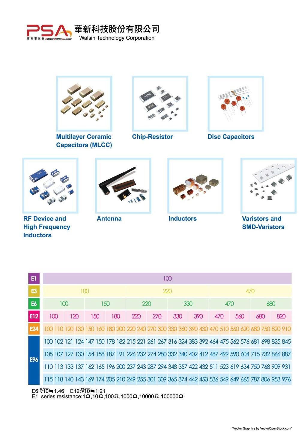
INDEX. How to Order Chip resistors Selection Guide General Purpose Chip Resistors ( 1Ω ~10MΩ )... 6
|
|
|
- Amber McKinney
- 5 years ago
- Views:
Transcription
1
2
3 Table of Contents Subject INDEX Page How to Order... 1 Chip resistors Selection Guide... 2 General Purpose ( 1Ω ~10MΩ )... 6 Thick Film Low Ohm/ Power Low Ohm ( 0.02Ω ~ 0.976Ω)... 7 Metal Low Ohm Current Sensing Chip resistors ( 0.001Ω ~ 0.050Ω)... 8 Chip Resistor Array:Convex Termination... 9 WA06W Chip Resistor Array 16P8R Chip Resistor Array:Concave Termination High Precision Thin Film Array WT04X Chip Resistor Network WA04P Chip Attenuator Special MR/SR Series of Automotive & Anti-Sulfuration WR_R Series of Total Lead Free WKxxM Series of Trimmable WKxxV Series of High Voltage WFxxP Series of High Power WKxxS series of Surge High Precision Test and Requirements Packing on Tape and Reel Footprint Design Storage and Handling Condition check with our sales representatives or product engineers before ordering. * This catalog has only typical specifications because there is no space for detailed specifications. Therefore,
4 Chip Resistor Selection Guide General Purpose Chip-R Series Size Rated Power * Tolerance Resistance WR25X 2512 (6432) 1W ±100 ±1% ±200 ±5% WR18X 1218 (3248) 1W ±100 ±1% ±200 ±5% WR20X 2010 (5025) ±100 ±1% ±200 ±5% WR10X 1210 (3225) 1/3W ±100 ±1% ±200 ±5% WR12X 1206 (3216) ±100 ±1% ±5% 1 ~ 10MΩ WR08X 0805 (2012) ±100 ±1% ±5% WR06X 0603 (1608) 1/10W ±100 ±1% ±5% WR04X 0402 (1005) 1/16W ±100 ±1% ±5% WR02X 0201 (0603) 1/20W ±200 ±1% ±200 ±5% WR01X (0402) 1/32W ±200 ±1% ±200 ±5% 4.7 ~ 1MΩ Remark: 1. Detailed resistance vs. TCR and ordering code please refer to specific specifications. 2. Jumper resistor is not designed for fusing applications, designers shall apply dedicate fusible resistor or standard fuse in application circuits. 3. WRxxW defines for ±1% < 10ohm or > 1Mohm. Thick Film Low Ohm Chip-R T : Thick film triple power WW25T 3W Series Size Rated Power Tolerance Resistance WW25X 0.015Ω ~ 0.976Ω 2512 (6432) 1W WW25W 0.010Ω ~ 0.100Ω ±1% 0.020Ω ~ 0.976Ω WW18X 1218 (3248) 1W ±5% 0.015Ω ~ 0.976Ω WW20X 0.020Ω ~ 0.976Ω 2010 (5025) WW20W 0.010Ω ~ 0.100Ω WW10X 1/3W 0.020Ω ~ 0.976Ω 1210 (3225) WW10W 0.020Ω ~ 0.100Ω WW12X 0.010Ω ~ 0.976Ω 1206 (3216) WW12W 1/3W 0.010Ω ~ 0.100Ω WW08X 0.020Ω ~ 0.976Ω 0805 (2012) WW08W 0.050Ω ~ 0.100Ω WW06X 1/10W 0.100Ω ~ 0.976Ω 0603 (1608) WW06W 0.010Ω ~ 0.100Ω B : Thin film TCR 3ppm C : Thin film TCR 2ppm WW04X 0402 (1005) 1/16W Remark: 1. Detailed resistance vs. TCR and ordering code please refer to specific specifications. 2. Resistance value will be changed by soldering condition and design of soldering pad, please design products in consideration of this change. Thick Film Power Low Ohm Chip-R MA: Array Automotive SA: Array Anti-Sulfur TA: Thin Film Array (Convex) Q : *2, TC50, convex R : *2, TC25, convex M : *4, TC50, convex N : *4, TC25, convex B : ± 0.1% C : ± 0.25% D : ± 0.5% Series Size Rated Power Tolerance Resistance WW25P 2512 (6432) 2W < 0.1Ω: 150ppm 0.1Ω: 100ppm 0.047Ω ~ 0.976Ω WW20P 2010 (5025) 1W < 0.1Ω: 150ppm 0.1Ω: 100ppm 0.047Ω ~ 0.976Ω WW10P 1210 (3225) < 0.1Ω: 500ppm 0.1Ω: 200ppm 0.020Ω ~ 0.976Ω WW12P 1206 (3216) < 0.1Ω: 200ppm 0.1Ω: 100ppm 0.020Ω ~ 0.976Ω WW08P 0805 (2012) 1/3W < 0.1Ω: 200ppm 0.1Ω: 150ppm 0.047Ω ~ 0.976Ω WW06P 0603 (1608) < 0.1Ω: 250ppm 0.1Ω: 200ppm 0.047Ω ~ 0.976Ω WW04P 0402 (1005) < 0.1Ω: 300ppm 0.1Ω: 200ppm 0.100Ω ~ 0.976Ω WW12C 1206 (3216) < 0.02Ω: 150ppm 0.02Ω: 100ppm 0.020Ω ~ 0.100Ω WW08C 0805 (2012) 1/3W < 0.03Ω: 200ppm 0.03Ω: 100ppm 0.010Ω ~ 0.100Ω WW06C 0603 (1608) < 0.051Ω: 0~+250ppm 0.051Ω: ±150ppm 0.010Ω ~ 0.100Ω WW04C 0402 (1005) < 0.051Ω: 0~+350ppm 0.051Ω: ±150ppm 0.025Ω ~ 0.100Ω WW02C 0201 (0603) 1/10W 0 ~ +500ppm ±5%: ~ 0.100Ω ±1%: ~ 0.100Ω 1 2
5 Metal Low Ohm Sensing Type Chip-R Series Size Rated Power * Tolerance Resistance WW59M 5931 (15079) 5W ±75 2, 3, 5, 10mΩ WW25A 3W ±70 5, 6, 8, 10, 18, 20, 25, 30, 35, 40, 50mΩ WW25N 2W ±70 3~10, 12,15, 20, 25, 30, 33, 35, 50, 100mΩ WW25R 2W ±70 1, 2, 3, 4, 5, 6, 7, 8, 9, 10mΩ 2512 (6432) 3, 4, 5, 6, 7, 8, 9, 10, WW25M 1W ±70 12, 15, 20, 25, 30, 33, 35, 50mΩ WW25Q 1W ±70 1, 2, 3, 4, 5, 6, 7, 8, 9, 10, 11, 12, 13, 14, 15mΩ WW20M 1/2 W ±70 5, 10, 15, 20mΩ 2010 (5025) WW20N 1W ±70 5, 10, 15, 20mΩ WW12M 1/2 W ±70 5, 10, 15, 20mΩ WW12N 1W ±70 5, 10, 15, 20, 25, 30mΩ 1206 (3216) WW12R 1W ±70 1 ~ 15mΩ WW12D 1W ±70 20, 25, 30, 40, 50mΩ WW08D ±70 20, 25, 30, 40, 50mΩ WW08R 0805 (2012) ±70 4, 5, 10mΩ WW08K ±100 5, 6, 7, 8, 9, 10mΩ WW06R 0603 (1608) 1/3W ±70 5, 10, 15mΩ Remark: 1. Detailed resistance vs. TCR and ordering code please refer to specific specifications. 2. Resistance value will be changed by soldering condition and design of soldering pad, please design products in consideration of this change. Chip Resistor Array Series Size Rated Power Termination Tolerance Resistance TA06N 0603x4 1/10W ±25 Convex 47~200KΩ ±0.1%, TA06M 0603x4 1/10W ±50 Convex ±0.5%, 47~200KΩ TA02R 0201x2 1/20W ±25 Convex ±0.25%, 10~10KΩ TA02Q 0201x2 1/20W ±50 Convex 10~10KΩ WA06X 1206 (0603x4) 1/10W ±200 Convex WA06T 1206 (0603x4) 1/10W ±200 Concave WA06Y 0606 (0603x2) 1/10W ±200 Convex WA04X 0804 (0402x4) 1/16W ±200 Convex WA04T 0804 (0402x4) 1/16W ±300 Concave WA04F 0804 (0402x4) 1/16W ±300 Reverse Concave WA04Y 0404 (0402x2) 1/16W ±200 Convex WA04U 0404 (0402x2) 1/16W ±300 Concave WA04G 0804 (0402x2) 1/16W ±300 Reverse Concave WA06W 1606 (0402x8) 1/16W ±200 Convex 10 ~ 100KΩ WA02A 0502 (0201x4) 1/32W ±200 Flat ±5%: ; WA02B 0202 (0201x2) 1/32W ±200 Flat ±1%: 10 ~ 100KΩ WA02F 0502 (0201x4) 1/32W ±200 Reverse Flat ±5%: ; WA02G 0202 (0201x2) 1/32W ±200 Reverse Flat ±1%: 10 ~ 100KΩ Remark: 1. Detailed resistance vs. TCR and ordering code please refer to specific specifications. 2. Resistance value will be changed by soldering condition and design of soldering pad, please design products in consideration of this change. Chip Attenuator Series Size Type Termination Tolerance Attenuation Impedance WA04P 0404 (0402x2) 4P3R, Π type Convex ±0.1dB ~ 2.5dB 0, 0.5dB ~ 20dB 50Ω Chip Resistor Network Series Size Rated Power Termination Tolerance Resistance WT04X 1206 (10P8R) 1/16W ±200 Convex ±5% 10 ~ 100KΩ High Power Chip-R Series Size Rated Power Tolerance Resistance WF25P 2512 (6432) 2W ±100 Jumper; 1 ~ 1MΩ WF20P 2010 (5025) 1W ±100 Jumper; 1 ~ 1MΩ WF10P 1210 (3225) ±100 Jumper; 1 ~ 1MΩ WF12P 1206 (3216) ±100 Jumper; 1 ~ 10MΩ WF08P 0805 (2012) ±100 Jumper; 1 ~ 10MΩ WF06P 0603 (1608) ±100 Jumper; 1 ~ 1MΩ WF04P 0402 (1005) ±100 Jumper; 1 ~ 1MΩ Surge Chip-R Series Size Rated Power TCR(ppm/ ) Tolerance Resistance WK25S 2512 (6432) 1W ~ 22MΩ WK20S 2010 (5025) 3/4W ~ 22MΩ WK10S 1210 (3225) 200 ±5%, ±10%, ±20% 0.27 ~ 22MΩ WK12S 1206 (3216) 1/3W ~ 22MΩ WK08S 0805 (2012) ~ 22MΩ WK06S 0603 (1608) ~10MΩ Automotive Chip-R ( Details please refer Automotive resistor introduction ) Series Size Rated Power TCR(ppm/ ) Tolerance Resistance MF12R 1206 (3216) 0.4W ±25 ±1%, 0.05%, 0.1%, 0.25%,0.5% 10Ω~ 1MΩ MF08R 0805 (2012) 0.25W ±25 ±1%, 0.05%, 0.1%, 0.25%,0.5% 10Ω~ 350KΩ MF06R 0603 (1608) 0.15W ±25 ±1%, 0.05%, 0.1%, 0.25%,0.5% 40Ω~ 130KΩ MF04R 0402 (1005) 0.062W ±25 ±1%, 0.05%, 0.1%, 0.25%,0.5% 40Ω~ 35KΩ MR (6432) 1W ±200 1~ 10MΩ MR (5025) ±200 1~ 10MΩ MR (3248) 1W ±200 1~ 10MΩ MR (3225) ±200 ± 1%, ±5% 1~ 10MΩ MR (3216) ±200 1~ 10MΩ MR (2012) ±200 1~ 10MΩ MR (1608) 1/10W ±200 1~ 10MΩ MR (1005) 1/16W ±200 1~ 10MΩ Anti-Sulfuration Chip-R ( Details please refer Anti-sulfur resistor introduction ) Series Size Rated Power TCR(ppm/ ) Tolerance Resistance SF12R 1206 (3216) ± 25 10Ω ~ 1MΩ SF08R 0805 (2012) ± 25 10Ω ~ 1MΩ SF06R 0603 (1608) 1/10W ± 25 ±0.05%, ±0.10%, 10Ω ~ 330KΩ SF12Q SF08Q 1206 (3216) 0805 (2012) ± 50 ± 50 ±0.25%, ±0.50%, ±1.0% 10Ω ~ 1MΩ 10Ω ~ 1MΩ SF06Q 0603 (1608) 1/10W ± 50 10Ω ~ 330KΩ SR (6432) 1W ± 200 1~ 10MΩ SR (5025) ± 200 1~ 10MΩ SR (3216) 200 1~ 10MΩ SR (2012) 200 1~ 10MΩ SR (1608) 1/10W 200 1~ 10MΩ SR (1005) 1/16W 200 1~ 10MΩ High Ohm Chip-R Series Size Rated Power TCR(ppm/ ) Tolerance Resistance WF12G 1206 (3216) M~100MΩ WF08G 0805 (2012) M~100MΩ WF06G 0603 (1608) 1/10W M~100MΩ WF04G 0402 (1005) 1/16W M~30MΩ High Voltage Chip-R Series Size Rated Power TCR(ppm/ ) Voltage (V) Tolerance Resistance WK25N 2512 (6432) 1W ±5%, ±10%, ±20% 4.7M ~ 16MΩ WK20N 2010 (5025) ±5%, ±10%, ±20% 1M ~ 16MΩ WK 2512 (6432) 1W ~ 51MΩ WK20V 2010 (5025) ~ 51MΩ WK12V 1206 (3216) ~ 51MΩ WK08V 0805 (2012) ~ 51MΩ WK06V 0603 (1608) 1/10W ~ 10MΩ Trimmable Chip-R Series Size Rated Power TCR(ppm/ ) Tolerance Resistance WK12M 1206 (3216) 200 0/-20%, 0/-30% 1 ~ 4.7MΩ WK08M 0805 (2012) 1/10W 200 0/-20%, 0/-30% 1 ~ 4.7MΩ WK06M 0603 (1608) 1/16W 100 0/-20%, 0/-30% 10~ 4.7MΩ Total lead free Chip-R ( Pb < 100ppm ) Series Size Rated Power TCR(ppm/ ) Tolerance Resistance WR25X_R 2512 (6432) 1W 200 1~ 10MΩ WR18X_R 1218 (3248) 1W 200 1~ 10MΩ WR20X_R 2010 (5025) 200 1~ 10MΩ WR10X_R 1210 (3225) 1/3W 200 1~ 10MΩ WR12X_R 1206 (3216) 200 1~ 10MΩ WR08X_R 0805 (2012) 200 1~ 10MΩ WR06X_R 0603 (1608) 1/10W 200 1~ 10MΩ WR04X_R 0402 (1005) 1/16W 200 1~ 10MΩ WR02X_R 0201 (0603) 1/20W 200 1~ 10MΩ WA04X_R 0402X4 1/16W 200 WA06X_R 0603X4 1/10W
 100 ±0.1%, ±0.5% WF06H 0603 (1608) 1/10W 100 ±0.1%, ±0.5% WF04H 0402 (1005) 1/16W 100 ±0.1%, ±0.5% WF25T 2512(6432) 3/4W ±50 ±0.01%, ±0.05%, ±0.10%,±0.25%, ±0.50%, ±1.0% 4.")
6 High Precision Chip-R Series Size Rated Power TCR(ppm/ ) Tolerance Resistance WF25H 2512 (6432) 1W 100 ±0.1%, ±0.5% WF20H 2010 (5025) 100 ±0.1%, ±0.5% WF10H 1210 (3225) 1/3W 100 ±0.1%, ±0.5% WF12H 1206 (3216) 100 ±0.1%, ±0.5% WF08H 0805 (2012) 100 ±0.1%, ±0.5% WF06H 0603 (1608) 1/10W 100 ±0.1%, ±0.5% WF04H 0402 (1005) 1/16W 100 ±0.1%, ±0.5% WF25T 2512(6432) 3/4W ±50 ±0.01%, ±0.05%, ±0.10%,±0.25%, ±0.50%, ±1.0% 4.7 ~ 3MΩ WF25Q 2512(6432) 1W ±50 ±0.01%, ±0.05%, ±0.10%,±0.25%, ±0.50%, ±1.0% 10 ~ 1.5MΩ WF20T 2010(5025) ±50 ±0.01%, ±0.05%, ±0.10%,±0.25%, ±0.50%, ±1.0% 4.7 ~ 3MΩ WF20Q 2010(5025) 3/4W ±50 ±0.01%, ±0.05%, ±0.10%,±0.25%, ±0.50%, ±1.0% 10 ~ 1.5MΩ WF10T 1210(3225) ±50 ±0.01%, ±0.05%, ±0.10%,±0.25%, ±0.50%, ±1.0% 4.7 ~ 2.49MΩ WF10Q 1210(3225) 2/5W ±50 ±0.01%, ±0.05%, ±0.10%,±0.25%, ±0.50%, ±1.0% WF12T 1206(3216) ±50 ±0.01%, ±0.05%, ±0.10%,±0.25%, ±0.50%, ±1.0% 4.7 ~ 2.49MΩ WF12Q 1206(3216) ±50 ±0.01%, ±0.05%, ±0.10%,±0.25%, ±0.50%, ±1.0% 4.7 ~ 1MΩ WF08T 0805(2012) 1/10W ±50 ±0.01%, ±0.05%, ±0.10%,±0.25%, ±0.50%, ±1.0% 4.7 ~ 2MΩ WF08Q 0805(2012) ±50 ±0.01%, ±0.05%, ±0.10%,±0.25%, ±0.50%, ±1.0% 4.7 ~ 1MΩ WF06T 0603 (1608) 1/16W ±50 ±0.01%, ±0.05%, ±0.10%,±0.25%, ±0.50%, ±1.0% 4.7 ~ 1MΩ WF06Q 0603 (1608) 1/10W ±50 ±0.01%, ±0.05%, ±0.10%,±0.25%, ±0.50%, ±1.0% 4.7 ~ 680KΩ WF04T 0402 (1005) 1/16W ±50 ±0.01%, ±0.05%, ±0.10%,±0.25%, ±0.50%, ±1.0% 10 ~ 255KΩ(~511KΩ*) WF04Q 0402 (1005) 1/10W ±50 ±0.01%, ±0.05%, ±0.10%,±0.25%, ±0.50%, ±1.0% 10 ~ 100KΩ WF02T 0201 (0603) 1/32W ±50 ±0.10%, ±0.5%, ±1.0% 100 ~ 12KΩ WF02Q 0201 (0603) 1/20W ±50 ±0.50%, ±1.0% 27 ~ 22KΩ WF25U 2512(6432) 3/4W ±25 ±0.01%, ±0.05%, ±0.10%,±0.25%, ±0.50%, ±1.0% 4.7 ~ 3MΩ WF25R 2512(6432) 1W ±25 ±0.01%, ±0.05%, ±0.10%,±0.25%, ±0.50%, ±1.0% 10 ~ 1.5MΩ WF20U 2010(5025) ±25 ±0.01%, ±0.05%, ±0.10%,±0.25%, ±0.50%, ±1.0% 4.7 ~ 3MΩ WF20R 2010(5025) 3/4W ±25 ±0.01%, ±0.05%, ±0.10%,±0.25%, ±0.50%, ±1.0% 10 ~ 1.5MΩ WF10U 1210(3225) ±25 ±0.01%, ±0.05%, ±0.10%,±0.25%, ±0.50%, ±1.0% 4.7 ~ 2.49MΩ WF10R 1210(3225) 2/5W ±25 ±0.01%, ±0.05%, ±0.10%,±0.25%, ±0.50%, ±1.0% WF12U 1206(3216) ±25 ±0.01%, ±0.05%, ±0.10%,±0.25%, ±0.50%, ±1.0% 4.7 ~ 2.49MΩ WF12R 1206(3216) ±25 ±0.01%, ±0.05%, ±0.10%,±0.25%, ±0.50%, ±1.0% 4.7 ~ 1MΩ WF08U 0805 (2012) 1/10W ±25 ±0.01%, ±0.05%, ±0.10%,±0.25%, ±0.50%, ±1.0% 4.7 ~ 2MΩ WF08R 0805 (2012) ±25 ±0.01%, ±0.05%, ±0.10%,±0.25%, ±0.50%, ±1.0% 4.7 ~ 1MΩ WF06U 0603 (1608) 1/16W ±25 ±0.01%, ±0.05%, ±0.10%,±0.25%, ±0.50%, ±1.0% 4.7 ~ 1MΩ WF06R 0603 (1608) 1/10W ±25 ±0.01%, ±0.05%, ±0.10%,±0.25%, ±0.50%, ±1.0% 4.7 ~ 680KΩ WF04U 0402 (1005) 1/16W ±25 ±0.01%, ±0.05%, ±0.10%,±0.25%, ±0.50%, ±1.0% 10 ~ 255KΩ(~511KΩ)* WF04R 0402 (1005) 1/10W ±25 ±0.01%, ±0.05%, ±0.10%,±0.25%, ±0.50%, ±1.0% 10 ~ 100KΩ WF02U 0201 (0603) 1/32W ±25 ±0.10%, ±0.5%, ±1.0% 100 ~ 12KΩ WF02R 0201 (0603) 1/20W ±25 ±0.50%, ±1.0% 27 ~12KΩ WF25F 2512(6432) 3/4W ±15 ±0.01%, ±0.05%, ±0.10%,±0.25%, ±0.50%, ±1.0% 4.7 ~ 1.5MΩ WF20F 2010(5025) ±15 ±0.01%, ±0.05%, ±0.10%,±0.25%, ±0.50%, ±1.0% 4.7 ~ 900KΩ(~1MΩ)* WF10F 1210(3225) ±15 ±0.01%, ±0.05%, ±0.10%,±0.25%, ±0.50%, ±1.0% 4.7 ~ 400KΩ(~1MΩ)* WF12F 1206(3216) ±15 ±0.01%, ±0.05%, ±0.10%,±0.25%, ±0.50%, ±1.0% 4.7 ~ 300KΩ(~1MΩ)* WF08F 0805(2012) ±15 ±0.01%, ±0.05%, ±0.10%,±0.25%, ±0.50%, ±1.0% 4.7 ~ 200KΩ(~1MΩ)* WF06F 0603 (1608) 1/10W ±15 ±0.01%, ±0.05%, ±0.10%,±0.25%, ±0.50%, ±1.0% 4.7 ~ 100KΩ(~511KΩ)* WF04F 0402 (1005) 1/16W ±15 ±0.01%, ±0.05%, ±0.10%,±0.25%, ±0.50%, ±1.0% 10 ~ 20KΩ(~69.8KΩ)* WF25W 2512(6432) 3/4W ±10 ±0.01%, ±0.05%, ±0.10%,±0.25%, ±0.50%, ±1.0% 4.7 ~ 1.5MΩ WF20W 2010(5025) ±10 ±0.01%, ±0.05%, ±0.10%,±0.25%, ±0.50%, ±1.0% 4.7 ~ 900KΩ WF10W 1210(3225) ±10 ±0.01%, ±0.05%, ±0.10%,±0.25%, ±0.50%, ±1.0% 4.7 ~ 400KΩ(~499KΩ)* WF12W 1206(3216) ±10 ±0.01%, ±0.05%, ±0.10%,±0.25%, ±0.50%, ±1.0% 4.7 ~ 300KΩ(~499KΩ)* WF08W 0805(2012) ±10 ±0.01%, ±0.05%, ±0.10%,±0.25%, ±0.50%, ±1.0% 4.7 ~ 200KΩ WF06W 0603 (1608) 1/10W ±10 ±0.01%, ±0.05%, ±0.10%,±0.25%, ±0.50%, ±1.0% 4.7 ~ 100KΩ(~332KΩ)* WF04W 0402 (1005) 1/16W ±10 ±0.01%, ±0.05%, ±0.10%,±0.25%, ±0.50%, ±1.0% 10 ~ 20KΩ(~60KΩ)* WF25Z 2512(6432) 3/4W ±5 ±0.01%, ±0.05%, ±0.10%,±0.25%, ±0.50%, ±1.0% 4.7 ~ 600KΩ WF20Z 2010(5025) ±5 ±0.01%, ±0.05%, ±0.10%,±0.25%, ±0.50%, ±1.0% 4.7 ~ 360KΩ WF10Z 1210(3225) ±5 ±0.01%, ±0.05%, ±0.10%,±0.25%, ±0.50%, ±1.0% 4.7 ~ 150KΩ WF12Z 1206(3216) ±5 ±0.01%, ±0.05%, ±0.10%,±0.25%, ±0.50%, ±1.0% 4.7 ~ 120KΩ WF08Z 0805(2012) ±5 ±0.01%, ±0.05%, ±0.10%,±0.25%, ±0.50%, ±1.0% 4.7 ~ 80KΩ WF06Z 0603 (1608) 1/10W ±5 ±0.01%, ±0.05%, ±0.10%,±0.25%, ±0.50%, ±1.0% 4.7 ~ 40KΩ WF04Z 0402 (1005) 1/16W ±5 ±0.01%, ±0.05%, ±0.10%,±0.25%, ±0.50%, ±1.0% 10 ~ 8KΩ WF25B 2512(6432) 3/4W ±3 ±0.01%, ±0.05%, ±0.10%,±0.25%, ±0.50%, ±1.0% 4.7 ~ 600KΩ WF20B 2010(5025) ±3 ±0.01%, ±0.05%, ±0.10%,±0.25%, ±0.50%, ±1.0% 4.7 ~ 360KΩ WF10B 1210(3225) ±3 ±0.01%, ±0.05%, ±0.10%,±0.25%, ±0.50%, ±1.0% 4.7 ~ 150KΩ WF12B 1206(3216) ±3 ±0.01%, ±0.05%, ±0.10%,±0.25%, ±0.50%, ±1.0% 4.7 ~ 120KΩ WF08B 0805(2012) ±3 ±0.01%, ±0.05%, ±0.10%,±0.25%, ±0.50%, ±1.0% 4.7 ~ 80KΩ WF06B 0603 (1608) 1/10W ±3 ±0.01%, ±0.05%, ±0.10%,±0.25%, ±0.50%, ±1.0% 4.7 ~ 40KΩ WF04B 0402 (1005) 1/16W ±3 ±0.01%, ±0.05%, ±0.10%,±0.25%, ±0.50%, ±1.0% 10 ~8KΩ* WF25C 2512(6432) 3/4W ±2 ±0.01%, ±0.05%, ±0.10%,±0.25%, ±0.50%, ±1.0% 4.7 ~ 600KΩ WF20C 2010(5025) ±2 ±0.01%, ±0.05%, ±0.10%,±0.25%, ±0.50%, ±1.0% 4.7 ~ 360KΩ WF10C 1210(3225) ±2 ±0.01%, ±0.05%, ±0.10%,±0.25%, ±0.50%, ±1.0% 4.7 ~ 150KΩ WF12C 1206(3216) ±2 ±0.01%, ±0.05%, ±0.10%,±0.25%, ±0.50%, ±1.0% 4.7 ~ 120KΩ WF08C 0805(2012) ±2 ±0.01%, ±0.05%, ±0.10%,±0.25%, ±0.50%, ±1.0% 4.7 ~ 80KΩ WF06C 0603 (1608) 1/10W ±2 ±0.01%, ±0.05%, ±0.10%,±0.25%, ±0.50%, ±1.0% 4.7 ~ 40KΩ WF04C 0402 (1005) 1/16W ±2 ±0.01%, ±0.05%, ±0.10%,±0.25%, ±0.50%, ±1.0% 10 ~8KΩ* * on request -200 ~ ~ +125 C 5 6

 passed on it. The sensing voltage be treated as a signal to trigger the switches (CMOS) ON/OFF duration so that to monitor and/or adjust the output current from inductor.")

 2010 (5025) 1218 (3248) 1210 (3225) ±5%, ±1% 0.020Ω ~ 0.976Ω 0.100Ω ~ 0.")
7 Thick Film Low Ohm/Power Low Ohm Function For Low Ohm The low ohmic resistors are used to sense output current in power supply, automotive and engine control management system, and other power sensing application. As shows in figure below, the typical function of low ohmic (power) chip resistor is to be a current sensor (Rsense) to generate the sensing voltage (Vs) for the purpose of feedback control when output current (lo) passed on it. The sensing voltage be treated as a signal to trigger the switches (CMOS) ON/OFF duration so that to monitor and/or adjust the output current from inductor. Simplify to say, Vs=Io Rsense. In general case, this feedback voltage is setting around 100mV for considering both on power saving and noise robustness. To sense a 5 ampere average output current, the Rsense resistance value therefore be required as 100mV / 5A = 20 mω, the power dissipation will be : P=I2 R =5A2 20mΩ =0.5Watt A low ohmic chip resistor with a power rating of 1.0 watt is recommended on this application in case the power safety margin is taken into account. of Low Ohm Chip Resistor Size code WW25X WW20X WW18X WW10X WW12X WW08X WW06X WW04X 2512 (6432) 2010 (5025) 1218 (3248) 1210 (3225) ±5%, ±1% 0.020Ω ~ 0.976Ω 0.100Ω ~ 0.976Ω 1206 (3216) 0805 (2012) Detailed TCR please refer to specific data sheets 1 Watt 0.5 Watt 1 Watt 1/3 Watt 1/4 Watt 1/8 Watt 1/10 Watt 1/16 Watt Max. Operation Voltage (DC or RMS) 2 100V JIS C / IEC This is the maximum voltage that may be continuously supplied to the resistor element, see IEC publication Power derating curve, and detail specification please refer to specific data sheets. 3. Resistance value will be changed by soldering condition and design of solding pad, please design products in consideration of change of resistance value. of Power Low Ohm Chip Resistor Item General Specification WW25P WW20P WW12P WW08P WW06P WW04P Size code 2512 (6432) 2010 (5025) 1206 (3216) 0805(2012) 0603(1608) 0402(1005) ±5%, ±1% 0.047Ω ~ 0.976Ω 0.1Ω~0.976Ω <0.100Ω ±150ppm/ ±150ppm/ ±200ppm/ ±200ppm/ ±250ppm/ Ω ±100ppm/ ±100ppm/ ±100ppm/ ±150ppm/ ±200ppm/ 0~+300ppm/ 2 W 1 W 1/2 W 1/3 W 1/4 W 1/8 W Max. Operation Voltage (DC or RMS) 300V 1. This is the maximum voltage that may be continuously supplied to the resistor element, see IEC publication Max. Operation Voltage : So called RCWW (Rated Continuous Working Voltage) is determined by RCWV= Rater Power Resistance Value or Max. RCWV listed above, whichever is lower. 3. 2W loading with total solder-pad and trace size of 300mm2 Physical Dimensions Dimensions WW25P WW20P WW12P WW08P WW06P WW04P L 6.30± ± ± ± ± ±0.05 W 3.10± ± ± ± ± ±0.05 T 0.60± ± ± ± ± ±0.05 Tt 0.60± ± ± ± ± ±0.10 Tb 1.80± ± ± ± ± / (1608) 0402 (1005) Metal Low Ohm Sensing (0.001Ω~ 0.050Ω) Description The resistors are constructed in a high grade low resistive metal body. The resistive layer is covered with a protective coat and printed a resistance marking code over it. Finally, the two external end terminations are added. For ease of soldering the outer layer of these end terminations is a lead free terminations. Item Item General Specification WW25M WW25N WW20M WW20N WW12N WW12M Size code 2512 (6432) 2010 (5025) 1206(3216) ±5%, ±1% 3, 5, 10, 12, 3, 5, 10,15, 20, 25mΩ 15, 20, 25, 50mΩ 5, 10, 15, 20mΩ 5, 10, 15, 20, 25mΩ 3mΩ: ±100ppm; > 3m: ±75ppm ± 75 ppm/ ± 70 ppm/ 1 W 2 W 1/2 W 1 W 1 W 1/2 W Max. Operation Voltage (DC or RMS) 2 2 Max. Overload Voltage (DC or RMS) 500V 500V 400V 1. This is the maximum voltage that may be continuously supplied to the resistor element, see IEC publication Power derating curve, and detail specification please refer to specific data sheets. 3. Resistance value will be changed by soldering condition and design of solding pad, please design products in consideration of chang of resistance value. Physical Dimensions: WW25M(0.002Ω~0.025Ω), WW25N(0.003Ω~0.025Ω), WW20N, WW12N Symbol L 6.40± ± ±0.20 W 3.20± ± ±0.20 T 0.60± ± ±0.25 Tt 0.65± ± ±0.20 Tb 0.65± ± ±0.20 WW25M(0.001Ω), WW25N(0.001Ω~0.002Ω) Symbol 2512 L 6.40±0.20 W 3.20±0.20 T 0.60±0.10 Tt 1.60±0.25 Tb 1.60±0.25 WW25Q, WW25R, WW12R, WW12D, WW06R 1. The detailed dimensions please refer to data sheet per type! General Specification WW25R WW25Q WW12R WW12D WW08R WW08D WW06R Size code 2512 (6432) 1206(3216) 0805 (2012) 0603 (1608) ±5%, ±1% 1,2,3,4,5,6 7,8,9,10mΩ 1 ~ 15mΩ 1 ~ 15mΩ 20, 25, 30, 40, 50mΩ 4, 5, 10mΩ 20, 25, 30, 40 50mΩ 5, 10, 15mΩ ±100ppm ±75ppm ±75ppm ±75ppm 2 W 1 W 1 W 1 W 1/2 W 1/2 W 1/3 W Max. Operation Current (DC or RMS) 44.7A 14A 11A 5A 8.1A 7 6 8


8 Array : Convex Termination Application 1. High reliability and stability 1. Consumer electrical equipment, PDA Digital Camcorder, 2. Reduced size of final equipment 2. EDP, Computer application 3. Lower assembly cost and higher surface mounted efficiency 3. Mobile phone, Telecom 4. Higher component and equipment reliability 4. DIMM Description and Physical Dimensions The resistors array is constructed in a high grade ceramic body (aluminum oxide). Internal metal electrodes are added at each end and connected by a resistive paste that is applied to the top surface of the substrate. The composition of the paste is adjusted to give the approximate resistance required and the value is trimmed to within tolerance by laser cutting of this resistive layer. The resistive layer is covered with a protective coat. Finally, the two external end terminations are added. For ease of soldering the outer layer of these end termination is Tin solder alloy. Marking code description is depended on component size and tolerance. Following figure shown the construction of a Chip-R array. WA06W Array 16P8R Description The resistors array is constructed in a high grade ceramic body (aluminum oxide). Internal metal electrodes are added at each end and connected by a resistive paste that is applied to the top surface of the substrate. The composition of the paste is adjusted to give the approximate resistance required and the value is trimmed to within tolerance by laser cutting of this resistive layer. The resistors layer is covered with a protective coat. Finally, the two external end terminations are added. For ease of soldering the outer layer of these end termination is Tin (Pb free) solder alloy. Item General Specification Physical Dimensions Type WA06X WA04X WA06Y WA04Y L 3.20± ± ± ±0.10 W 1.60± ± ± ±0.10 T 0.50± ± ± ±0.10 P 0.80± ± ± ±0.10 A 0.60± ± ± ±0.10 B 0.30± ± ± ±0.15 C 0.40± ± G 0.30± ± ± ±0.17 WA06W WA06W_N Size 1606 (0602 8) 1606 (0602 8) Termination construction Convex type Convex type ±5% (E24 series) ±5% (E24 series) 10Ω~100KΩ, Jumper (0Ω) 10Ω~100KΩ, Jumper (0Ω) ± 200 ppm/ ± 200 ppm/ 1/16 W 1/16 W Max. Operation Voltage (DC or RMS) Max. Overload Voltage (DC or RMS) 100V Carrier Tape width 12mm 8mm WA06X WA04X WA06Y WA04Y Size (1608 4) (1005 4) (1608 4) (1005 2) Termination construction 8P4R,Convex 4P2R,Convex Circuit Mode: R1=R2=R3=R4=R5=R6=R7=R8 ±5%, ±1% (E24 series) 10Ω~1MΩ(E24 series), Jumper (0Ω) ±200 ppm/ 1/10 Watt 1/16 Watt 1/10 Watt 1/16 Watt Power derating curve and detail specification please refer to specific data sheets. Physical Dimensions: Max. Operation Voltage (DC or RMS) Max. Overload Voltage (DC or RMS) 100V 100V 100V Circuit Mode: R1=R2(=R3=R4) Symbol WA06W WA06W_N L 4.00± ±0.10 W 1.60± ±0.10 T 0.45± ±0.10 B 0.30± ±0.10 G 0.30± ±0.10 D 0.20± ±0.10 P 0.50± ±0.10 H1 0.40± ±0.10 H2 0.30± ±0.10 Power derating curve and detail specification please refer to specific data sheets


.")
9 Array : Concave Termination Application 1. High reliability and stability 1. Consumer electrical equipment, PDA Digital Camcorder, 2. Reduced size of final equipment 2. EDP, Computer application 3. Lower assembly cost and higher surface mounted efficiency 3. Mobile phone, Telecom 4. Higher component and equipment reliability 4. DIMM 5. Strong body and terminations 6. Excellent performance in surface mounting assembly. High Precision Thin Film Array 1. SMD metal film resistor 2. High reliability and stability of 0.1% and below per customer request 3. High performance of TCR: 25 ppm/k and below per customer request 4. Low current noise Application 1. Medical equipment 2. Measuring instrument 3. Communication device 4. Computer Description and Physical Dimensions The resistor array is constructed in a high grade ceramic body (aluminum oxide). Internal metal electrodes are added at each end and connected by a resistive paste that is applied to the top surface of the substrate. The composition of the paste is adjusted to give the approximate resistance required and the value is trimmed to within tolerance by laser cutting of this resistive layer. The resistive layer is covered with a protective coat. Finally, the two external end terminations are added. For ease of soldering the outer layer of these end termination is Tin solder alloy. Marking code description is depended on component size and tolerance. Following figure shown the construction of a Chip-R array. Description The resistors are constructed in a high grade ceramic body (aluminum oxide). Internal metal electrodes are added at each end and connected by a resistive layer that is applied to the top surface of the substrate. The composition of the resistive layer is adjusted to give the approximate resistance required and the value is trimmed to nominated value within tolerance which controlled by laser trimming of this resistive layer. The resistive layer is covered with a protective coat. Finally, the two external end terminations are added. For environmental soldering issue, the outer layer of these end terminations is a Lead-free solder. Item General Specification WA06T WA04T WA04U Size (1608 4) (1005 4) (1005 2) Termination construction Concave type ±5%, ±1% (E24 series) 10Ω~1MΩ, Jumper (0Ω) ± 200 ppm/ ± 300 ppm/ ± 300 ppm/ 1/10 W 1/16 W 1/16 W Max. Operation Voltage (DC or RMS) Max. Overload Voltage 100V Physical Dimensions: Type TA06N/TA06M TA02R/TA02Q W 1.50 ± ± 0.10 L 3.20 ± ± 0.10 P 0.80 ± ± 0.10 C 0.40 ± ± 0.10 A 0.60 ± ± 0.10 B 0.30 ± G 0.25 ± T ± ± 0.10 TA06N TA06M TA02R TA02Q Size 0603x4 0201x2 Termination construction 8P4R,Convex 4P2R,Convex ±0.5%, ±0.25%, ±0.1% (E24 + E192 series) ±25 ppm/ ±50 ppm/ ±25 ppm/ ±50 ppm/ Circuit Mode 47 ~ 200KΩ 1/10W 10 ~ 10KΩ 1/20W Max. Operation Voltage (DC or RMS) 75V 15V L /-0.10mm 2.00±0.10mm 1.00±0.10mm W /-0.10mm 1.00±0.10mm 1.00±0.10mm T 0.60±0.20mm 0.45±0.10mm 0.30±0.10mm P 0.80±0.10mm 0.50±0.05mm 0.50±0.05mm A 0.60±0.15mm 0.35±0.05mm 0.35±0.10mm B 0.35±0.15mm 0.20±0.15mm 0.25±0.15mm C 0.50±0.15mm 0.25±0.05mm 0.35±0.10mm G 0.50±0.15mm 0.25±0.15mm 0.25±0.15mm 1. Power derating curve and detail specification please refer to specific data sheets. 2. Max. Operation Voltage : So called RCWW (Rated Continuous Working Voltage) is determined by RCWV = Rater Power Resistance Value or Max. RCWV listed above, whichever is lower. Max. Overload Voltage -55 ~ +155 JIS C / IEC Power derating curve and detail specification please refer to specific data sheets. 30V 11 12


 General Specification WT04X 0402x8 (1005x8) Convex type ±5% (E24 series) 10Ω ~ 100KΩ ± 200 ppm/ 1/16 W WA04P Chip Attenuator Typical Application of Chip Attenuator WA04")
10 WT04X Chip Resistor Network 10P8R Description The resistor array is constructed in a high grade ceramic body (aluminum oxide). Internal metal electrodes are added at each end and connected by a resistive paste that is applied to the top surface of the substrate. The composition of the paste is adjusted to give the approximate resistance required and the value is trimmed to within tolerance by laser cutting of this resistive layer. The resistive layer is covered with a protective coat. Finally, the two external end terminations are added. For ease of soldering the outer layer of these end termination is Tin (Pb free) solder alloy. Size Termination construction Item Max. Operation Voltage (DC or RMS) General Specification WT04X 0402x8 (1005x8) Convex type ±5% (E24 series) 10Ω ~ 100KΩ ± 200 ppm/ 1/16 W WA04P Chip Attenuator Typical Application of Chip Attenuator WA04 P 001 X B T L Size code WA04: 0402 per element Type code P: convex, π type attenuator Attenuation Range 000 = 0dB R05 = 0.5dB 001 = 1dB R15 = 1,5dB 002 = 2dB 003 = 3dB 004 = 4dB 005 = 5dB 006 = 6dB 007 = 7dB 008 = 8dB 009 = 9dB 010 =10dB 011 = 11dB 012 = 12dB 013 = 13dB 014 = 14dB 015 = 15dB 016 = 16dB 017 = 17dB 018 = 18dB 019 = 19dB 020 = 20dB Characteristic Impedance X:50Ω π type Attenuator for VSWR improvement and output frequency level matching on VCO application. Attenuation Tolerance A : ± 0.1dB B : ± 0.3dB C : ± 0.4dB D : ± 0.8dB E : ± 1.0dB F : ± 1.5dB G : ± 2.0dB H : ± 2.5dB P : - Termination T=7'' reel taped Packaging L=Sn base (lead free) Max. Overload Voltage (DC or RMS) Circuit Mode: Resistor elements on pin1 ~ pin4, pin6 ~ pin9; R1=R2=R3=R4=R6=R7=R8=R9 1. Power derating curve and detail specification please refer to specific data sheets. Physical Dimensions: Symbol L 3.30±0.20 W 1.60±0.15 T 0.55±0.10 P 0.64±0.05 A 0.50±0.05 B 0.40±0.15 C 0.40±0.15 G 0.40±0.15 Physical Dimensions: WA04P L 1.00±0.10 W /-0 T 0.35±0.10 P 0.65±0.20 A 0.33±0.10 Ta 0.15±0.10 Tb 0.25±0.10 Item General Specification WA04P Size (1005 2) Termination construction Attenuation Range Attenuation Tolerance 0dB 0.5dB 1dB~ 5dB 6dB~ 10dB 11dB~ 13dB 14dB 15dB~ 16dB 17dB~ 19dB 20dB Characteristic impedance Rated power at Tamb=70 Limiting Voltage (DC) Frequency range (DC) Convex type 0dB, 0.5dB ~ 20dB - ± 0.1dB ± 0.3dB ± 0.4dB ± 0.8dB ± 1.0dB ± 1.5dB ± 2.0dB ± 2.5dB 50Ω 0.1 W / package MAX. 3 GHz VSWR (Voltage Standing Wave Ratio) MAX. 1.2 Number of Resistors Number of Terminals 3 resistors 4 terminals -40 ~ 125 C
 to fulfill RoHS environmental regulation. 3. Provided trimmable resistors (WKxxM series) for customer special tolerance requirement. 4.")
11 Special Application 1. Provided Automotive & Anti-sulfuration resistors (MR/SR series) for Auto & Anti-sulfuration application. 2. Provided Total Lead Free resistors (WR_R series) to fulfill RoHS environmental regulation. 3. Provided trimmable resistors (WKxxM series) for customer special tolerance requirement. 4. Provided high precision tolerance (WFxxH/ WFxxT/ WFxxU/ WFxxW) down to ±0.05% and TCR down to 10ppm/ for voltage sensing application. 5. High reliability and stability. 6. Reduced size of final equipment 7. Lower assembly costs. 8. Higher component and equipment reliability 9. Special resistance, tolerance are available upon customer's request. MR/SR Series of Automotive & Anti-sulfuration Chip Resistor 1. High reliability and stability ±1%. 2. Sulfuration resistant 3. Automotive grade AEC Q-200 compliant % CCD inspection. 5. RoHS compliant and lead free. Size code *MR series can withstand H2S 3ppm 1000hrs. *SR series can withstand H2S 1000ppm 720hrs. WR_R Series of Total Lead Free 1. High reliability and stability 2. Reduced size of final equipment 3. Lower assembly cost 4. Higher component and equipment reliability 5. RoHS compliant and total lead free Size code Part No. Definition Application 1. Automotive application. 2. Consumer electrical equipment. 3. EDP, Computer application. 4. Telecom Application. 1 st code 2 nd code 3 rd ~ 4 th code 5 th code 6 th ~ 9 th code 10 th code 11 th code 12 th code R WTC Type code Size code Functional code For example: W R 04 Marking code (Resistance) 1Ω~10MΩ (±1%, ±5%),Jumper ±200 ppm* Max. Operation Voltage (DC or RMS) Max. Operation Voltage Size code Max. Operation Voltage Remark: *Detail specification please refer to specific data sheets! Remark: *Detail specification please refer to specific data sheets! MR25X 2512(6432) 1W 2 SR25X 2512(6432) 1W 2 WR10_R 1210(3225) 1/3 W MR20X 2010(5025) 1Ω~10MΩ (±1%, ±5%),Jumper ±200 ppm* SR20X 2010(5025) 1/2 W WR12_R 1206(3216) 1/4 W MR18X 1218(3248) 1W MR10X 1210(3225) SR12X 1206(3126) 1/4 W WR08_R 0805(2012) 1/8 W MR12X 1206(3126) 1/4 W WR06_R 0603(1608) 1/10 W Tolerance code Packaging code Termination code X 1000 F T R SR08X 0805(2012) 1Ω~10MΩ (±1%, ±5%),Jumper ±200 ppm* 1/8 W MR08X 0805(2012) 1/8 W SR06X 0603(1608) 1/10 W 75V WR04_R 0402(1005) 1/16 W MR06X 0603(1608) 1Ω~10MΩ (±1%, ±5%),Jumper ±200 ppm* 1/10 W 75V MR04X 0402(1005) 1/16 W WR02_R 0201(0603) 1/20 W SR04X 0402(1005) 1/16 W -55 ~ +125 C WKxxM Series of Trimmable 1. High precision, reliability and stability 2. Miniature size down to (1608) Description Application The resistors are constructed on a high grade ceramic body (aluminum oxide). Internal metal electrodes are added at each end and connected by a resistive paste that is applied to the top surface of the substrate. The composition of the paste is adjusted to give the approximate resistance required. The resistive layer is covered with a transparent protective coat. Finally, the two external end terminations are added. For ease of soldering the outer layer of these end termination is Tin (Pb free) solder alloy. Physical Dimensions Type WK25M WK20M WK10M WK12M WK08M WK06M L 6.30± ± ± ± ± ±0.10 W 3.20± ± ± ± ± /-0.10 T 0.55± ± ± ± ± ±0.10 Tb 0.60± ± ± ± ± ±0.10 Tt 0.60± ± ± ± ± ± Automotive application. 2. Consumer electrical equipment. 3. EDP, Computer application. 4. Telecom Application. WK25M WK20M WK10M WK12M WK08M WK06M Size code 2512 (6332) 2010 (5025) 1210(3225) 1206(3216) 0805(2012) 0603(1608) 0/-20%(Y) and 0/-30%(X) E24 series 1Ω ~ 4.7MΩ 10Ω ~ 4.7MΩ 10Ω ~ 4.7MΩ: ±200 ppm/ 1Ω ~ 9.1Ω: ~ +500 ppm/ ±200 ppm/ 1 W 1/2 W 1/4 W 1/8 W 1/10 W 1/16 W Max. Operation Voltage (DC or RMS) JIS C / IEC WKxxV Series of High Voltage 1. Special material and design for high working voltage required 2. Compatible with flow and reflow soldering. 3. Suitable for lead free soldering. Size code Max. Operation Voltage (DC or RMS) 1. This is the maximum voltage that may be continuously supplied to the resistor element, see IEC publication Max. Operation Voltage : So called RCWW (Rated Continuous Working Voltage) is determined by RCWV= Rater Power Resistance Value or Max. RCWV listed above, whichever is lower. Physical Dimensions Symbol L W T Tt Tb WK25N 6.30± ± ± ± ±0.20 WK20N 5.00± ± ± ± ±0.20 WK 6.30± ± ± ± ±0.20 WK20V 5.00± ± ± ± ±0.20 WK25N 2512 (6332) 4.7MΩ ~ 16MΩ 1 W 2000V WK12V 3.10± ± ± ± ±0.25 ±5% ; ±10% WK20N 2010 (5025) 1MΩ ~ 16MΩ 1500V WK08V 2.00± ± ± ± ± ~ +125 C Application 1. Power supply. 2. Automotive industry. 3. Measurement instrument. 4. Back light inverter. 5. Medical or Military equipment WK 2512 (6332) 47Ω ~ 51MΩ ± 200 ppm/ * detail refer to data sheet 1 W 800V WK06V 1.60± / ± ± ±0.10 WK20V 2010 (5025) 1/2 W 500V -55 ~ +125 C WK12V 1206(3216) ±5% ; ±1% 1/4 W 500V WK08V 0805(2012) 1/8 W 400V WK06V 0603(1608) 47Ω ~ 10MΩ 1/10 W

12 WFxxP Series of High Power 1. High power rating and compact size 2. High reliability and stability 3. Reduced size of final equipment 4. Lead free product is upon customer requested Item Application 1. Power supply 2. PDA 3. Digital meter 4. Computer 5. Automotives. General Specification WF25P WF20P WF10P WF12P WF08P WF06P WF04P Size code 2512(6432) 2010(5025) 1210(3225) 1206(3216) 0805(2012) 0603 (1608) 0402(1005) ±1%, ±5% 0Ω, 1Ω ~ 1MΩ ± 100 ppm/ 2W 1W Max. Operation Voltage (DC or RMS) 300V 1. This is the maximum voltage that may be continuously supplied to the resistor element, see IEC publication Max. Operation Voltage : So called RCWW (Rated Continuous Working Voltage) is determined by RCWV= Rater Power Resistance Value or Max. RCWV listed above, whichever is lower. 3. 2W loading with total solder-pad and trace size of 300mm Ω maximum resistance Rmax<15mΩ and rated current<4amp Physical Dimensions Symbol WF25P WF20P WF10P WF12P WF08P WF06P WF04P L 6.30± ± ± ± ± ± ±0.05 W 3.10± ± ± ± ± ± ±0.05 T 0.60± ± ± ± ± ± ±0.05 Tt 0.60± ± ± ± ± ± ±0.10 Tb 1.80± ± ± ± ± ± ±0.10 WKxxS Series of Anti-Surge 1. Power rating and compact size 2. High reliability and stability 3. Reduced size of final equipment 4. Surge protection Item General Specification Application WK25S WK20S WK10S WK12S WK08S Size code 2512(6432) 2010(5025) 1210(3225) 1206(3216) 0805(2012) ±5%,±10%,±20%,(E24) 0.27Ω ~ 22MΩ ± 200 ppm/ 1 W 3/4W Max. Operation Voltage (DC or RMS) 1. This is the maximum voltage that may be continuously supplied to the resistor element, see IEC publication Max. Operation Voltage : So called RCWV (Rated Continuous Working Voltage) is determined by RCWV= Rater Power Resistance Value or Max. RCWV listed above, whichever is lower. Physical Dimensions 1. Power supply. 2. Measurement instrument. 3. Automotive industry. 4. Medical or Military equipment. Symbol WK25S WK20S WK10S WK12S WK08S L 6.30± ± ± ± ±0.10 W 3.20± ± ± ± ±0.10 T 0.55± ± ± ± ±0.10 Tt 0.30± ± ± ± ±0.20 Tb 0.60± ± ± ± ±0.20 Power (W) Pulse chart of WKxxS series Duration (msec) High Precision Narrow Tolerance Thick Film TC100 WFxxH Series (E96+E24 series) WF12H WF08H WF06H WF04H Size 1206(3216) 0805(2012) 0603(1608) 0402(1005) ±0.5%, ±0.1% 10Ω ~ 1MΩ (E96+E24 series) ±100 ppm/ 1/4 W 1/8 W 1/10 W 1/16 W Max. Operation Voltage (DC or RMS) 100V (Detail specification please refer to specific data sheets) Narrow Tolerance Thin Film TC50 WFxxT/ WFxxQ Series (E192+E24 series) WF25T Size 2512(6432) 4.7 ~3MΩ 4.7 ~ 2.49MΩ 4.7 ~ 2MΩ 4.7 ~ 1MΩ 3/4W Max. Operation Voltage (DC or RMS) WF25Q WF20Q WF10Q WF12Q WF08Q WF06Q WF04Q WF02Q Size 2512(6432) 2010(5025) 1210(3225) 1206(3216) 0805(2012) 0603(1608) 0402(1005) 0201(0603) ±1%, ±0.5%, ±0.1%, ±0.05%, ±0.01% ±0.05%, ±1% 10 ~1.5MΩ 4.7 ~ 1MΩ 4.7 ~ 680KΩ 10 ~ 100KΩ 27 ~ 22KΩ ±50 ppm/ 1W 3/4W 2/5W 1/10W 1/10W 1/20W Max. Operation Voltage (DC or RMS) 75V 15V (Detail specification please refer to specific data sheets) * on request Narrow Tolerance Thin Film TC25 WFxxU/ WFxxR Series (E192+E24 series) WF25U Size 2512(6432) 4.7 ~3MΩ 4.7 ~ 2.49MΩ 4.7 ~ 2MΩ 4.7 ~ 1MΩ 3/4W Max. Operation Voltage (DC or RMS) WF25R WF20R WF10R WF12R WF08R WF06R WF04R WF02R Size 2512(6432) 2010(5025) 1210(3225) 1206(3216) 0805(2012) 0603(1608) 0402(1005) 0201(0603) ±1%, ±0.5%, ±0.1%, ±0.05%, ±0.01% ±0.05%, ±1% 10 ~1.5MΩ 4.7 ~ 1MΩ 4.7 ~ 680KΩ 10 ~ 100KΩ 27 ~ 12KΩ ±25 ppm/ 1W 3/4W 2/5W 1/10W 1/10W 1/20W Max. Operation Voltage (DC or RMS) 75V 15V (Detail specification please refer to specific data sheets) * on request WF20T 2010(5025) WF20U 2010(5025) Narrow Tolerance Thin Film TC15 WFxxF Series (E192+E24 series) WF25F Size 2512(6432) 4.7 ~ 1.5MΩ 3/4W Max. Operation Voltage (DC or RMS) (Detail specification please refer to specific data sheets) * on request WF20F 2010(5025) 4.7 ~ 900KΩ (~1MΩ)* WF10T WF12T WF08T WF06T WF04T WF02T 1210(3225) 1206(3216) 0805(2012) 0603(1608) 0402(1005) 0201(0603) ±1%, ±0.5%, ±0.1%, ±0.05%, ±0.01% ±0.1%, ±0.5%, ±1% 10 ~ 255KΩ (~511KΩ)* 100 ~ 12KΩ ±50 ppm/ WF10U WF12U WF08U WF06U WF04U WF02U 1210(3225) 1206(3216) 0805(2012) 0603(1608) 0402(1005) 0201(0603) ±1%, ±0.5%, ±0.1%, ±0.05%, ±0.01% ±0.1%, ±0.5%, ±1% 10 ~ 255KΩ (~511KΩ)* 100 ~ 12KΩ ±25 ppm/ 1/10W 100V 1/10W 100V 1/16W 1/16W WF10F WF12F WF08F 1210(3225) 1206(3216) 0805(2012) ±1%, ±0.5%, ±0.1%, ±0.05%, ±0.01% 4.7 ~ 400KΩ (~1MΩ)* 4.7 ~ 300KΩ (~1MΩ)* 4.7 ~ 200KΩ (~1MΩ)* ±15 ppm/ 100V 1/16W 1/16W WF06F 0603(1608) 4.7 ~ 100KΩ (~511KΩ)* 1/10W 1/32W 15V 1/32W 15V WF04F 0402(1005) 10 ~ 20KΩ (~69.8KΩ)* 1/16W 17 18
13 High Precision Narrow Tolerance Thin Film TC10 WFxxW Series (E192+E24 series) WF25W WF20W Size 2512(6432) 2010(5025) 4.7 ~ 1.5MΩ 4.7 ~ 900KΩ 3/4W Max. Operation Voltage (DC or RMS) * on request (Detail specification please refer to specific data sheets) WF10W WF12W WF08W 1210(3225) 1206(3216) 0805(2012) ±1%, ±0.5%, ±0.1%, ±0.05%, ±0.01% 4.7 ~ 400KΩ (~499KΩ)* 4.7 ~ 300KΩ (~499KΩ)* 4.7 ~ 200KΩ ±10 ppm/ Narrow Tolerance Thin Film TC5 WFxxZ Series (E192+E24 series) 100V WF06W 0603(1608) 4.7 ~ 100KΩ (~332KΩ)* 1/10W WF04W 0402(1005) 10 ~ 20KΩ (~60KΩ)* WF25Z WF20Z WF10Z WF12Z WF08Z WF06Z WF04Z Size 2512(6432) 2010(5025) 1210(3225) 1206(3216) 0805(2012) 0603(1608) 0402(1005) ±1%, ±0.5%, ±0.1%, ±0.05%, ±0.01% 4.7 ~ 600KΩ 4.7 ~ 360KΩ 4.7 ~ 150KΩ 4.7 ~ 120KΩ 4.7 ~ 80KΩ 4.7 ~ 40KΩ 10 ~ 8KΩ ±5 ppm/ 3/4W 1/10W 1/16W Max. Operation Voltage (DC or RMS) 100V (Detail specification please refer to specific data sheets) Narrow Tolerance Thin Film TC3 WFxxB Series (E192+E24 series) WF25B WF20B WF10B WF12B WF08B WF06B WF04B Size 2512(6432) 2010(5025) 1210(3225) 1206(3216) 0805(2012) 0603(1608) 0402(1005) ±1%, ±0.5%, ±0.1%, ±0.05%, ±0.01% 4.7 ~ 600KΩ 4.7 ~ 360KΩ 4.7 ~ 150KΩ 4.7 ~ 120KΩ 4.7 ~ 80KΩ 4.7 ~ 40KΩ 10 ~ 8KΩ* ±3 ppm/ 3/4W 1/10W 1/16W Max. Operation Voltage (DC or RMS) 100V * on request (Detail specification please refer to specific data sheets) Narrow Tolerance Thin Film TC2 WFxxC Series (E192+E24 series) WF25C WF20C WF10C WF12C WF08C WF06C WF04C Size 2512(6432) 2010(5025) 1210(3225) 1206(3216) 0805(2012) 0603(1608) 0402(1005) ±1%, ±0.5%, ±0.1%, ±0.05%, ±0.01% 4.7 ~ 600KΩ 4.7 ~ 360KΩ 4.7 ~ 150KΩ 4.7 ~ 120KΩ 4.7 ~ 80KΩ 4.7 ~ 40KΩ 10 ~ 8KΩ* ±2 ppm/ 3/4W 1/10W 1/16W Max. Operation Voltage (DC or RMS) 100V * on request (Detail specification please refer to specific data sheets) 1/16W Test and Requirements For WR Series Requirements Test Procedure / Test Method Resistor 0Ω - DC resistance values measurement - Temperature Coefficient of Resistance (T.C.R) Electrical Characteristics Natural resistance change per change in degree centigrade. Within the specified tolerance Refer JISC5201-1: 1998 Clause 4.8 [(R2-R1)/R1(T2-T1)] 10 6 (ppm / ) T1: to QUICK REFERENCE DATA <50mΩ R1:Resistance at reference temperature (20 +5 /-1 ) R2:Resistance at test temperature (-55 or +155 ) Resistance to soldering heat(r.s.h) ±5%: R/Rmax. (1%+0.05Ω) Un-mounted chips completely immersed for 10±1second in a SAC ±1%: R/Rmax. (0.5%+0.05Ω) solder bath at 260 ±5ºC Clause 4.18 no visible damage <50mΩ Solder ability Un-mounted chips completely immersed for 2±0.5 second in a SAC 95% coverage min., good tinning and no visible solder bath at 235 ±5 damage Clause 4.17 Temperature cycling ±5%: R/Rmax. (1%+0.05Ω) 30minutes at -55 ±3, 2~3minutes at ,30minutes at ±1%: R/Rmax. (0.5%+0.05Ω) +155 ±3,2~3minutes at ,total 5continuous cycles Clause 4.19 no visible damage <50mΩ High Temperature Exposure ±5%: R/Rmax. (2%+0.1Ω) /-0 hours; without load in a temperature chamber controlled 155 MIL-STD-202 ±1%: R/Rmax. (1%+0.1Ω) ±3 Mothod 108 no visible damage <50mΩ Bending strength ±5%: R/Rmax. (1%+0.05Ω) Resistors mounted on a 90mm glass epoxy resin PCB(FR-4), bending ±1%: R/Rmax. (1%+0.05Ω) once 3mm for 10sec, 5mm for WR04 Clause 4.33 no visible damage <50mΩ Adhesion No remarkable damage or removal of the Pressurizing force: 5N, Test time: 10±1sec. Clause 4.32 terminations Short Time Overload (STOL) ±5%: R/Rmax. (2%+0.1Ω) Clause times RCWV or max. overload voltage, for 5seconds ±1%: R/Rmax. (1%+0.1Ω) no visible damage <50mΩ Special Application of Automotive Thin Film MFxxR Series (E192+E24 series) MF12R MF08R MF06R MF04R Size 1206(3216) 0805(2012) 0603(1608) 0402(1005) ±0.5%, ±0.25%, ±0.1%, ±0.05% 10 ~ 350KΩ 40 ~ 130KΩ 40 ~ 35KΩ ±25 ppm/ 0.4W 0.25W 0.15W 0.062W Max. Operation Voltage (DC or RMS) 100V 75V / AEC Q200 / ASTM B Automotive grade AEC Q200 compliant. (Detail specification please refer to specific data sheets) Special Application of Anti-Sulfuration Thin Film SFxxQ/R Series (E96+E24 series) SF12Q SF08Q SF06Q SF12R SF08R SF06R Size 1206(3216) 0805(2012) 0603(1608) 1206(3216) 0805(2012) 0603(1608) ±1.0%, ±0.5%, ±0.25%, ±0.1%, ±0.05% 10 ~ 330KΩ 10 ~ 330KΩ ±50 ppm/ ±25 ppm/ 1/10W 1/10W Max. Operation Voltage (DC or RMS) 75V 75V / ASTM B-809 (Detail specification please refer to specific data sheets) Load life in Humidity Clause 4.24 Load life (endurance) Clause 4.25 Insulation Resistance Clause 4.6 Dielectric Withstand Voltage Clause /-0 hours, loaded with RCWV or Vmax in humidity chamber ±5%: R/Rmax. (2%+0.1Ω) controller 40 ±2 at and 90~95% relative humidity, 1.5 hours on and ±1%: R/Rmax. (1%+0.1Ω) 0.5 hours off no visible damage ±5%: R/Rmax. (2%+0.1Ω) /-0 hours, loaded with RCWV or Vmax in chamber controller 70 ±1%: R/Rmax. (1%+0.1Ω) ±2 1.5 hours on and 0.5 hours off no visible damage Apply the maximum overload voltage (DC) for 1minute R 10GΩ Apply the maximum overload voltage (AC) for 1minute No breakdown or flashover <50mΩ <50mΩ 19 20
 Natural resistance change per change in degree centigrade.")
![[(R2-R1)/R1(T2-T1)] 10 6 (ppm/ ) T1:20 +5-1 R1:Resistance at referance temperature (20 +5 /-1 ) Requirements Resistor Within the specified tolerance Refer to QUICK REFERENCE DATA Paper Tape](/docs-images/90/101824646/images/14-2.jpg "Specifications for WR,WF,WW Series and WA,WT Series Component Size / Series W F E PO ΦD 1210, 1206, 0805, 0603, 0402, WA06X, WA06T, WA04X, WA04Y, 8.00±0.30 3.50±0.")
14 For WW Series Packing on Tape and Reel: All specifications are in accordance with IEC ! Test Electrical Characteristics JISC5201-1: 1998 Clause 4.8 Procedure / Test Method - DC resistance values measurement - Temperature Coefficient of Resistance (T.C.R) Natural resistance change per change in degree centigrade. [(R2-R1)/R1(T2-T1)] 10 6 (ppm/ ) T1: R1:Resistance at referance temperature (20 +5 /-1 ) Requirements Resistor Within the specified tolerance Refer to QUICK REFERENCE DATA Paper Tape Specifications for WR,WF,WW Series and WA,WT Series Component Size / Series W F E PO ΦD 1210, 1206, 0805, 0603, 0402, WA06X, WA06T, WA04X, WA04Y, 8.00± ±0.20 WA04P, WA04T, WA04U, WT04X WA06W 12.0± ±0.05 WR02X 8.00± ± ± ±0.10 Φ R2:Resistance at test temperature (-55 or +155 ) Component Size / Series A B P1 T Resistance to soldering heat(r.s.h) Clause 4.18 Solder ability Clause 4.17 Temperature cycling Clause 4.19 High Temperature Exposure MIL-STD-202 Method 108 Bending strength Clause 4.33 Adhesion Clause 4.32 Un-mounted chips completely immersed for 10±1second in a SAC solder bath at 260 ±5ºC Un-mounted chips completely immersed for 2±0.5 second in a SAC solder bath at 235 ±5 30minutes at -55 ±3, 2~3minutes at ,30minutes at +155 ±3,2~3minutes at ,total 5continuous cycles /-0 hours; without load in a temperature chamber controlled 155 ±3 Resistors mounted on a 90mm glass epoxy resin PCB(FR-4), bending once 3mm for 10sec, 5mm for WR04 Pressurizing force: 5N, Test time: 10±1sec. R/R max. ±(1%+0.005Ω) no visible damge 95% coverage min., good tinning and no visible damage R/R max. ±(1%+0.005Ω) no visible damge R/R max. ±(3%+0.005Ω) no visible damge R/R max. ±(1%+0.005Ω) no visible damge No remarkable damage or removal of the terminations 1206(3216), WA06X, WA06T 3.60± ± (2012) 2.40± ± ±0.10 Max (1608) 1.90± ± ± (1005) 1.20± ± ± ±0.05 WA04X, WA04T 2.20± ± ±0.05 Max. 0.6 WA04Y, WA04P, WA04U 1.15± ± ± ±0.05 WT04X / / ± ±0.05 WA06W / / ± ±0.05 WR02X 0.67± ± ± ± (3225) 3.60± ± ±0.10 Max. 1.0 Plastic Tape Specifications for WR, WF, WW Series of Chip-R Component Size 2512(6432) 2010(5025) 1218(3248) A 6.90± ± ±0.30 B 3.60± ± ±0.20 W 12.00±0.30 F 5.50±0.10 E 1.75±0.10 P1 4.00± ±0.10 P0 4.00±0.10 ΦD Φ T Max. 1.2 Short Time Overload (STOL) Clause 4.13 Load life in Humidity Clause times RCWV or max. overload voltage, for 5 seconds /-0 hours, loaded with RCWV or Vmax in humidity chamber controller 40 ±2 at and 90~95% relative humidity, 1.5 hours on and 0.5 hours off R/R max. ±(2%+0.005Ω) no visible damge R/R max. ±(3%+0.005Ω) no visible damge Plastic Tape Reel Specifications for WR, WF, WW Series of Chip-R Reel/Tape A B C D 7 reel for 8mm tape 9.00±0.50 Φ178.0±0.20 Φ60.0± ± reel for 12mm tape 12.4± reel for 8mm tape Φ254.0±2.00 Φ100.0± ± ± reel for 12mm tape Φ254.0±2.00 Φ100.0± ± ± reel for 8mm tape Φ330.0±2.00 Φ100.0± ± ±0.50 Load life (endurance) Clause 4.25 Insulation Resistance Clause 4.6 Dielectric Withstand Voltage Clause /-0 hours, loaded with RCWV or Vmax in chamber controller R/R max. ±(3%+0.005Ω) 70 ±2 1.5 hours on and 0.5 hours off no visible damge Apply the maximum overload voltage (DC) for 1minute R 10GΩ Apply the maximum overload voltage (AC) for 1minute No breakdown or flashover Reel Taping Quantity Specifications for WR,WF,WW Series and WA,WT Series Component Size / Series Q'ty per reel Reel Diameter 0603, 0805, ,000 pcs 4 reel 1210, 1206, 0805, 0603, WA06X, WA06T, WT04X 5,000 pcs 7 reel 0201,0402, WA04X, WA04Y, WA04P, WA04T, WA04U 10,000 pcs 7 reel 0201, ,000 pcs 7 reel WA06X, WA06Y 5,000 pcs 7 reel 2512, ,000 pcs 7 reel ,000 pcs 10 reel 1206, 0805, 0603, WA06X, WA06T 10,000 pcs 10 reel 0201, 0402, WA04X, WA04Y Q: 20,000 pcs/ J: 40,000 pcs 10 reel 2010, ,000 pcs 10 reel 0201 H: 50,000 pcs/ G: 70,000 pcs 13 reel 0402 H: 50,000 pcs/ G: 70,000 pcs 13 reel WA04X, WA04Y 40,000 pcs 13 reel 1206, 0805, 0603, WA06X, 20,000 pcs 13 reel 2010, ,000 pcs 13 reel 21 22
15 Footprint Design Footprint Design for WRxx, WFxx, WWxx Series : Size Reflow Soldering Processing Remarks A B C D E F G Placement Accuracy ± ± ± ± ±0.25 IR or hot plate soldering ± ± ± ± ±0.25 Size Wave Soldering Processing Number & Dimensions A B C D E F G of dummy tracks Placement Accuracy ( ) ± ( ) ± ( ) ± ( ) ± ( ) ± ( ) ± ( ) ±0.25 Storage and Handling Conditions: 1. Products are recommended to be used up within two years since production as ensured shelf life. Check solderability in case shelf life extension is needed. 2. To store products with following condition: Temperature :5 to 40 Humidity : 20 to 70% relative humidity 3. Caution: a. Don't store products in a corrosive environment such as sulfide, chloride gas, or acid. It may cause oxidization of electrode, which easily be resulted in poor soldering b. To store products on the shelf and avoid exposure to moisture. c. Don't expose products to excessive shock, vibration, direct sunlight and so on Precaution of Soldering 1. It is recommended to use a mildly activated rosin flux ( less than 0.1% wt chlorine ) 2. Excessive flux must be avoided 3. When water-soluble flux is used, enough washing is necessary 4. Two times limitations for reflow soldering is highly recommended Recommendation of Soldering Profiles: 5. Solder repair by soldering iron a. Max. 350 for below 3 seconds is highly recommended b. Do not directly contact termination to avoid thermal shock. 6. Prevent any external force on the products until solder is cooled Mounting 1. Imperfect adjustment of mounting machine may cause the cracks, the chipping and the alignment error. Check and inspect the mounting machine in advance. 2. Set the backup pins in proper layout otherwise the components mounted on the backside of the board are damaged. Do not set these pins at the position of the nozzle. 3. Adjust the bottom dead point of dispenser away from the board when you apply adhesive. 4. Confirm that the products are corresponding to flow soldering when you perform it. 5. Pay attention to the amount of solder because improper amount of solder place large stress on the products and cause cracks or malfunctions. Washing 1. Confirm the ionic residues in solder do not remain after washing for moisture resistance and corrosion. Resistance may cause deterioration when these substances are attached to the products. 2. Confirm the reliability in advance when using no washing solder, water or soluble agent. 3. Wash thoroughly after soldering to remove ionic substances like sweat and salinity. 4. The ultrasonic washing may destruct the products due to resonance by vibration. High hydraulic pressure may also damage the products. 5. Dry the products sufficiently after washing. In general application, the lead free (Pb-free) termination CRs are used and may be mounted on PCB by IR reflow or wave soldering process with lead-free solder material. The recommended soldering profiles are shown as Fig.1 & 2. The lead-free termination CRs are also suitable on SMT process against lead-containing solder paste. But the soldering temperature should be higher than the melting point of solder paste 30 at least. If the optimized solder joint is requested, increasing soldering time, temperature and concentration of N2 within oven are recommended. Advised IR reflow soldering profile is shown as Fig.3. Symbol 0603x4 array 0603x2 array 0402x4 array 0402x2 array 0402x8 array WA02A WA02B / / ± ± ± ± ± ± ± ± / / / / ± ± ± ± / ± ± ± ± / / ± ± ±0.10 Footprint Design for 10P8R Network Resistor : Symbol WT04X W1 0.50±0.05 W2 0.35±0.05 H2 0.80±0.10 P1 0.70±0.05 P2 0.65±0.05 A 3.20±0.10 F / Fig. 1 Recommended IR reflow soldering profile for SMT process with SnAgCu series solder paste 3-5 sec Fig. 2 Recommended wave soldering profile for SMT process with SnAgCu series solder 23 Fig. 3 Recommended reflow soldering profile for SMT process with eutectic SnPb solder paste. Fig. 4 Recommended soldering profile by manual with SnAgCu series solder material 24
16 PLAN & MEMO PLAN & MEMO 25 26
17 PLAN & MEMO 27
18

19
INDEX. How to Order Chip resistors Selection Guide General Purpose Chip Resistors ( 1Ω ~10MΩ )... 6
... 6") Table of Contents Subject INDEX Page How to Order... 1 Chip resistors Selection Guide... 2 General Purpose ( 1Ω ~10MΩ )... 6 Thick Film Low Ohm/ Power Low Ohm ( 0.02Ω ~ 0.976Ω)... 7 Metal Low Ohm Current
Table of Contents Subject INDEX Page How to Order... 1 Chip resistors Selection Guide... 2 General Purpose ( 1Ω ~10MΩ )... 6 Thick Film Low Ohm/ Power Low Ohm ( 0.02Ω ~ 0.976Ω)... 7 Metal Low Ohm Current
High Power Low Ohm Chip Resistors. Size W, W, /2W
 WW25P, WW20P, WW12P ±1%, ±5% 47mΩ~976mΩ High Power Low Ohm Chip Resistors Size 2512 2W, 2010 1W, 1206 1/2W *Contents in this sheet are subject to change without prior notice. Page 1 of 7 ASC_WW25P-20P-12P_V08
WK25S WK20S WK10S WK12S WK08S WK06S. Thick Film Power Surge Chip Resistors. Size 2512, 2010, 1210, 1206, 0805, 0603
 WK25S WK20S WK10S WK12S WK08S WK06S ±5% 5%, ±10 10%, ±20 20% Thick Film Power Surge Chip Resistors Size 2512, 2010, 1210, 1206, 0805, 0603 *Contents in this sheet are subject to change without prior notice.
WF10H ±0.1%, ±0.5% High Precision chip resistors Size 1210
 WF10H ±0.1%, ±0.5% High Precision chip resistors Size 1210 *Contents in this sheet are subject to change without prior notice. Page 1 of 7 ASC_WF10H_V01 Jan.2010 FEATURE 1. High reliability and stability
WF08P, WF06P. High Power Chip Resistors Size /4W ; /8W. Customer : Approval No : Issue Date : Customer Approval :
 WF08P, WF06P ±1%, ±5% 0Ω, 1Ω~1MΩ High Power Chip Resistors Size 0805 1/4W ; 0603 1/8W Customer : Approval No : Issue Date : Customer Approval : Page 1 of 7 WF08P;WF06P Version 04 Jul.-2009 FEATURE 1. Small
WK25S WK20S WK10S WK12S WK08S WK06S. Thick Film Power Surge Chip Resistors AEC Q-200 Qualified Size 2512, 2010, 1210, 1206, 0805, 0603
 WK25S WK20S WK10S WK12S WK08S WK06S ±5% 5%, ±10 10%, ±20 20% Thick Film Power Surge Chip Resistors AEC Q-200 Qualified Size 2512, 2010, 1210, 1206, 0805, 0603 *Contents in this sheet are subject to change
1 7 ASC_WF06A_V01 NOV
 WF06A 1 ~ 1Mohm ±5%, ±1% High Power Chip Resistors Size 0603 1/4W *Contents in this sheet are subject to change without prior notice. Page 1 of 7 ASC_WF06A_V01 NOV - 2015 FEATURE 1. Small size and light
WK25S WK20S WK10S WK12S WK08S. Thick Film Power Surge Chip Resistors. Size 2512, 2010, 1210, 1206, 0805
 WK25S WK20S WK10S WK12S WK08S ±5%, ±10%, ±20% Thick Film Power Surge Chip Resistors Size 2512, 2010, 1210, 1206, 0805 *Contents in this sheet are subject to change without prior notice. Page 1 of 7 ASC_WKxxS_V02
WF25S WF20S WF12S ±5% 20% Power Surge Chip Resistors Size 2512, 2010, Customer : Approval No : Issue Date : Customer Approval :
 WF25S WF20S WF12S ±5% 5%, ±10 10%, ±20 20% Power Surge Chip Resistors Size 2512, 2010, 1206 Customer : Approval No : Issue Date : Customer Approval : Page 1 of 7 WF25S WF20S WF12S Ver.4 Sep.-2008 FEATURE
High Power Chip Resistors Size W, W, /2W
 WF25P, WF20P, WF12P ±1%, ±5% 0Ω,1Ω~1MΩ High Power Chip Resistors Size 2512 2W, 2010 1W, 1206 1/2W Customer : Approval No : Issue Date : Customer Approval : Page 1 of 7 WF25P, WF20P, WF12P, Ver.8 Jul.2010
WF12H, WF08H, WF06H, WF04H ±0.1% High precision chip resistors Size 1206, 0805, 0603, 0402
 WF12H, WF08H, WF06H, WF04H ±0.1% High precision chip resistors Size 1206, 0805, 0603, 0402 Customer : Approval No : Issue Date : Customer Approval : Page 1 of 7 WFxxHB ±0.1% Ver.13 Sep.-2008 FEATURE 1.
WW25W, WW20W, WW10W, WW12W, WW08W, WW06W
 WW25W, WW20W, WW10W, WW12W, WW08W, WW06W ±1%, ±5% Thick Film Power Low Ohm Chip Resistors RoHS Exemption free and Lead free Size 2512, 2010, 1210, 1206, 0805, 0603 *Contents in this sheet are subject to
WF12H, WF08H, WF06H, WF04H ±0.5% High precision chip resistors Size 1206, 0805, 0603, 0402
 WF12H, WF08H, WF06H, WF04H ±0.5% High precision chip resistors Size 1206, 0805, 0603, 0402 Customer : Approval No : Issue Date : Customer Approval : Page 1 of 7 WFxxHD ±0.5% Ver.13 March.-2010 FEATURE
SPECIFICATION SHEET. ±1%, ±5%, Convex Type General purpose chip resistors array
 SPECIFICATION SHEET CNA24, CNA34 ±1%, ±5%, Convex Type General purpose chip resistors array Size 0402x4, 0603x4 (8p4R) ( Automotive & Anti-sulfur ) All data in this sheet are subject to change, modify
WR18X(W), WR20X(W), WR25X(W) ±1%, ±5% Power chip resistors Size 1218,2010,2512
, WR20X(W), WR25X(W) ±1%, ±5% Power chip resistors Size 1218,2010,2512") WR18X(W), WR20X(W), WR25X(W) ±1%, ±5% Power chip resistors Size 1218,2010,2512 Customer : Approval No : Issue Date : Customer Approval : Page 1 of 7 WR18-20-25X(W) Ver.13 Oct.-2010 FEATURE 1. High power
WR18X(W), WR20X(W), WR25X(W) ±1%, ±5% Power chip resistors Size 1218,2010,2512 Customer : Approval No : Issue Date : Customer Approval : Page 1 of 7 WR18-20-25X(W) Ver.13 Oct.-2010 FEATURE 1. High power
WT04X ±5%, Convex Type 10p8R Chip resistors network Size 1206
 WT04X ±5%, Convex Type 10p8R Chip resistors network Size 1206 Customer : Approval No : Issue Date : Customer Approval : Page 1 of 7 WT04X Ver.13 Sep.-2008 FEATURE 1. Small size and light weight 2. Reduced
WR10, WR12, WR08, WR06, WR04 ±1%, ±5% General purpose chip resistors. Size 1210, 1206, 0805, 0603, 0402
 WR10, WR12, WR08, WR06, WR04, General purpose chip resistors Size 1210, 1206, 0805, 0603, 0402 ( Automotive & Anti-sulfuration ) *Contents in this sheet are subject to change without prior notice. Page
Thick Film General purpose chip resistors
 WR02X(W) ±5%, ±1% Thick Film General purpose chip resistors Size 0201 *Contents in this sheet are subject to change without prior notice. Page 1 of 7 ASC_WR02X_V18 MAY - 2016 FEATURE 1. Small size and
WA04T ±5%, ±1% Concave Type General purpose chip resistors array
 WA04T ±5%, ±1% Concave Type General purpose chip resistors array Size 0402x4 *Contents in this sheet are subject to change without prior notice. Page 1 of 7 ASC_WA04T_Concave_V10 Oct.2010 FEATURE 1. Small
SR20X, SR25X ±1%, ±5% Power chip resistors Size 2010, 2512
 SR20X, SR25X ±1%, ±5% Power chip resistors Size 2010, 2512 ( Automotive & Anti-sulfuration ) Page 1 of 7 SR20-25X_V04 Sep.-2011 FEATURE 1. High reliability and stability ±1% 2. Sulfuration resistant 1000ppm
WA04X, WA06X ±1%, ±5%, Convex Type General purpose chip resistors array
 WA04X, WA06X ±1%, ±5%, Convex Type General purpose chip resistors array Size 0402x4, 0603x4 (8p4R) (Automotive ) Page 1 of 8 ASC_WAxxX_J_V05 May.2011 FEATURE 1. Small size and light weight 2. Reduced size
WW12W ±1%, ±5% Size W. Thick Film High Power Low Ohm Chip Resistors. Approval sheet
 ±1%, ±5% Thick Film High Power Low Ohm Chip Resistors Size 1206 1W *Contents in this sheet are subject to change without prior notice. Page 1 of 6 ASC 1W TC200_V01 DEC - 2015 FEATURE 1. High power rating
WR10X ±1%, ±5% General purpose chip resistors Size 1210
 WR10X ±1%, ±5% General purpose chip resistors Size 1210 Customer : Approval No : Issue Date : Customer Approval : Page 1 of 7 WR10X Version 02 Jun.-2005 FEATURE 1. High reliability and stability 2. Reduced
MA04X, MA06X ±1%, ±5%, Convex Type General purpose chip resistors array
 MA04X, MA06X ±1%, ±5%, Convex Type General purpose chip resistors array Size 0402x4, 0603x4 (8p4R) ( Automotive & Anti-sulfur ) Page 1 of 8 MA04/ 06_V03 Apr.2010 FEATURE 1. High reliability and stability
WR12, WR08, WR06, WR04 ±1%, ±5% General purpose chip resistors. Size 1206, 0805, 0603, ( Automotive )
") WR12, WR08, WR06, WR04 ±1%, ±5% General purpose chip resistors Size 1206, 0805, 0603, 0402 ( Automotive ) Page 1 of 9 WR_J(AUTO)_ V03 Sep.2010 FEATURE 1. Automotive grade AEC Q-200 compliant 2. 100% CCD
WR12, WR08, WR06, WR04 ±1%, ±5% General purpose chip resistors Size 1206, 0805, 0603, 0402 ( Automotive ) Page 1 of 9 WR_J(AUTO)_ V03 Sep.2010 FEATURE 1. Automotive grade AEC Q-200 compliant 2. 100% CCD
WA04X ±5%, Convex Type General purpose chip resistors array Size 0402x4
 WA04X ±5%, Convex Type General purpose chip resistors array Size 0402x4 Customer : Approval No : Issue Date : Customer Approval : Page 1 of 7 WA04X Version 20 Sep.-2008 FEATURE 1. Small size and light
WF20M / WF12M / WF08M / WF06M 0/-20% and 0/-30% Trimmable chip resistors
 WF20M / WF12M / WF08M / WF06M 0/-20% and 0/-30% Trimmable chip resistors Size 2010, 1206, 0805, 0603 Page 1 of 7 WFxxM Trimmable_V11 Apr.2010 FEATURE 1. Reduced size of final equipment 2. Lower assembly
WW25X ±1%, ±5% Low ohmic power chip resistors Size 2512
 WW25X ±1%, ±5% Low ohmic power chip resistors Size 2512 Customer : Approval No : Issue Date : Customer Approval : Page 1 of 7 WW25X Version 06 Jul.-2004 FEATURE 1. High power rating and compact size 2.
WA04, WA06 ±1%, ±5%, Convex Type & Concave Type General purpose chip resistors array
 WA04, WA06 ±1%, ±5%, Convex Type & Concave Type General purpose chip resistors array Size 0402x2 (4p2R) Size 0402x4, 0603x4 (8p4R) Size 0602x8 (16p8R) *Contents in this sheet are subject to change without
Size 1206, 1210, 0805, 0603, 0402 (Anti-Sulfuration )
") SR12, SR10, SR08, SR06, SR04, General purpose chip resistors Size 1206, 1210, 0805, 0603, 0402 (Anti-Sulfuration ) *Contents in this sheet are subject to change without prior notice. Page 1 of 9 ASC_SR_V03
SR12, SR10, SR08, SR06, SR04, General purpose chip resistors Size 1206, 1210, 0805, 0603, 0402 (Anti-Sulfuration ) *Contents in this sheet are subject to change without prior notice. Page 1 of 9 ASC_SR_V03
Thick Film Chip Resistors
 Description: The resistors are constructed in a high grade ceramic body (aluminum oxide). Internal metal electrodes are added at each end and connected by a resistive paste that is applied to the top surface
WR02X(W) ±5%, ±1% RoHS compliant and Lead content 100ppm General purpose chip resistors Size 0201
 ±5%, ±1% RoHS compliant and Lead content 100ppm General purpose chip resistors Size 0201") WR02X(W) ±5%, ±1% RoHS compliant and Lead content 100ppm General purpose chip resistors Size 0201 *Contents in this sheet are subject to change without prior notice. Page 1 of 7 ASC_WR02X_TR_V02 Jul -
WR02X(W) ±5%, ±1% RoHS compliant and Lead content 100ppm General purpose chip resistors Size 0201 *Contents in this sheet are subject to change without prior notice. Page 1 of 7 ASC_WR02X_TR_V02 Jul -
WA04X ±5%, Convex Type General purpose chip resistors array Size 0402x4
 WA04X ±5%, Convex Type General purpose chip resistors array Size 0402x4 Customer : Approval No : Issue Date : Customer Approval : Page 1 of 8 WA04X Version 15 Sept.-2004 FEATURE 1. Small size and light
WW25X, WW18X, WW12X, WW08X, WW06X ±1%, ±5% Thick Film Current Sensing Chip Resistors Size 2512, 1218, 1206, 0805, 0603 (Automotive)
") WW25X, WW18X, WW12X, WW08X, WW06X ±1%, ±5% Thick Film Current Sensing Chip Resistors Size 2512, 1218, 1206, 0805, 0603 (Automotive) *Contents in this sheet are subject to change without prior notice. Page
WW25X, WW18X, WW12X, WW08X, WW06X ±1%, ±5% Thick Film Current Sensing Chip Resistors Size 2512, 1218, 1206, 0805, 0603 (Automotive) *Contents in this sheet are subject to change without prior notice. Page
WR04X ±1%, ±5% General purpose chip resistors Size 0402
 WR04X ±1%, ±5% General purpose chip resistors Size 0402 Customer : Approval No : Issue Date : Customer Approval : Page 1 of 7 WR04X Version 14 Jul.-2007 FEATURE 1. Small size and light weight 2. High reliability
WW12M, WW12N ±1%, ±5%, 1/2W, 1W Ultra low ohmic power chip resistors
 WW12M, WW12N ±1%, ±5%, 1/2W, 1W Ultra low ohmic power chip resistors Size 1206 (3216) Sensing Type *Contents in this sheet are subject to change without prior notice. Page 1 of 7 ASC_WW12MN_V05 Jul.2010
WR18, WR20, WR25 ±1%, ±5% Power chip resistors Size 1218,2010,2512
 WR18, WR20, WR25 ±1%, ±5% Power chip resistors Size 1218,2010,2512 Customer : Approval No : Issue Date : Customer Approval : Page 1 of 7 WR18, WR20, WR25 Version 3 Oct.-2004 FEATURE 1. High power rating
WW25N ±1%, ±5%, 2W Ultra low ohm power chip resistors Size 2512 (6432)
") WW25N ±1%, ±5%, 2W Ultra low ohm power chip resistors Size 2512 (6432) Metal Current Sensing Type *Contents in this sheet are subject to change without prior notice. Page 1 of 7 ASC_WW25N_V14 Jul - 2015
WW25N ±1%, ±5%, 2W Ultra low ohm power chip resistors Size 2512 (6432) Metal Current Sensing Type *Contents in this sheet are subject to change without prior notice. Page 1 of 7 ASC_WW25N_V14 Jul - 2015
WR02X ±5%, ±1% General purpose chip resistors Size 0201
 WR02X ±5%, ±1% General purpose chip resistors Size 0201 Customer : Approval No : Issue Date : Customer Approval : Page 1 of 8 WR02X Version 03 Jul.-2004 FEATURE 1. Small size and light weight 2. High reliability
High Power Chip Resistor
 Description: The resistors are constructed in a high grade ceramic body (aluminium oxide). Internal metal electrodes are added at each end and connected by a resistive paste that is applied to the top
WF12SR360JTL. Size Surge 5% chip resistors. Customer : Approval No : Issue Date : Customer Approval :
 SPECIFICATION OF SURGE 5% CHIP RESISTOR Ver: 1 Page: 1 of 7 ROHS compliance WF12SR360JTL Surge 5% chip resistors Size 1206 Customer : Approval No : Issue Date : Customer Approval : SPECIFICATION OF SURGE
INDEX. How to Order Chip Resistors Selection Guide... 2~ Chip Resistors Array : Convex Termination...
 INDEX Subject Page How to Order.... 1 Chip Resistors Selection Guide... 2~3... 4... 5.... Chip Resistors Array : Convex ermination....... Chip Resistors Array : Concave ermination........... 11 Special
WF06P 5% High power chip resistors Size 0603, 1/8watt
 SPECIFICATION OF HIGH POWER CHIP RESISTOR Ver: 1 Page: 1 of 7 ROHS compliance WF06P 5% High power chip resistors Size 0603, 1/8watt Customer : Approval No : Issue Date : Customer Approval : SPECIFICATION
Thick Film Low Ohm Chip Resistors
 Description: The resistors are constructed in a high grade ceramic body (aluminium oxide). Internal metal electrodes are added at each end and connected by a resistive paste that is applied to the top
WW25M 1%, 5% Metal Plate Low Ohm Power Chip Resistors. Size 2512 (6432) 1W Current Sensing Type RoHS Exemption free and Halogen free
 1W Current Sensing Type RoHS Exemption free and Halogen free") WW25M 1%, 5% Metal Plate Low Ohm Power Chip Resistors Size 2512 (6432) 1W Current Sensing Type RoHS Exemption free and Halogen free *Contents in this sheet are subject to change without prior notice. Page
WW25M 1%, 5% Metal Plate Low Ohm Power Chip Resistors Size 2512 (6432) 1W Current Sensing Type RoHS Exemption free and Halogen free *Contents in this sheet are subject to change without prior notice. Page
Surface Mount Thick Film Resistor MCWR Series
 Description The lead free resistors are constructed in a high grade ceramic body (aluminium oxide). Internal metal electrodes are added at each end and connected by a lead free resistive paste that is
1 8 WK L_V_AUTO_V01 FEB
 WK12L, WK20L, WK25L 1%, 5% Thick Film Power Chip Resistor Wide Termination RoHS compliant and Halogen free Size 0612, 1020, 1225 Automotive AEC Q200 Compliant ASTM B-809-95 Compliant *Contents in this
Automotive and Anti-Sulfuration Chip Resistor 0603
 The resistors are constructed in a high grade ceramic body (aluminium oxide). Internal metal electrodes are added at each end and connected by a resistive paste that is applied to the top surface of the
WR12X / WR08X / WR06X ±1%, ±5% General purpose chip resistors Size 1206 / 0805 / 0603
 WR12X / WR08X / WR06X ±1%, ±5% General purpose chip resistors Size 1206 / 0805 / 0603 Customer : Approval No : Issue Date : Customer Approval : Page 1 of 8 WR12X / WR08X / WR06X Version 17 Jul.-2004 FEATURE
Thin Film Chip Resistor (ARG Series)
") Construction D1 L (ARG Series) Features -Advanced thin film technology -SMD Type designed for automatic insertion -Wide resistance range 1ohm ~ 2.49Mega ohm Applications -Medical Equipment -Testing / Measurement
Construction D1 L (ARG Series) Features -Advanced thin film technology -SMD Type designed for automatic insertion -Wide resistance range 1ohm ~ 2.49Mega ohm Applications -Medical Equipment -Testing / Measurement
DATA SHEET CURRENT SENSOR - LOW TCR PT series 5%, 2%, 1% sizes 0402/0603/0805/1206/2010/2512
 DATA SHEET CURRENT SENSOR - LOW TCR PT series 5%, 2%, 1% sizes 0402/0603/0805/1206/2010/2512 RoHS compliant & Halogen free Product specification December 30, 2015 V.1 Product specification 2 SCOPE This
Thin Film Anti-Sulfurated Chip Resistor (TAS Series)
") (TAS Series) Features - Special materials, design, and processing for high sulfur applications - Tolerances as low as 0.05% and s as low as 10 ppm. - Test proven immunity to humidity, moisture, and sulfur
(TAS Series) Features - Special materials, design, and processing for high sulfur applications - Tolerances as low as 0.05% and s as low as 10 ppm. - Test proven immunity to humidity, moisture, and sulfur
Metal Alloy Low-Resistance Resistor Specifications
 Page 1 of 14 Metal Alloy Low-Resistance Resistor Specifications March 2010 Specification Number:GCT-SPEC-011-11 Issued Date:2010/03/01 Page 2 of 14 1. Scope: 1.1 This specification is covered following
1 Alumina Substrate 5 External Electrode (Sn) 2 Bottom Electrode (Ag) 6 Resistor Layer (RuO 2 ) 3 Top Electrode (Ag/Pd) 7 Primary Overcoat (Glass)
 2 Bottom Electrode (Ag) 6 Resistor Layer (RuO 2 ) 3 Top Electrode (Ag/Pd) 7 Primary Overcoat (Glass)") Thick Film Chip Resistor CR Series Construction 1 Alumina Substrate 5 External Electrode (Sn) 2 Bottom Electrode (Ag) 6 Resistor Layer (RuO 2 ) 3 Top Electrode (Ag/Pd) 7 Primary Overcoat (Glass) 4 Barrier
Thick Film Chip Resistor CR Series Construction 1 Alumina Substrate 5 External Electrode (Sn) 2 Bottom Electrode (Ag) 6 Resistor Layer (RuO 2 ) 3 Top Electrode (Ag/Pd) 7 Primary Overcoat (Glass) 4 Barrier
Metal Film Leaded Precision Resistor
 Features Excellent overall stability Very tight tolerance down to ±0.05% Extremely low TCR down to ±5 PPM/ C High power rating up to 3 Watts Excellent ohmic contact Applications Automotive Telecommunication
1 Alumina Substrate 5 External Electrode (Sn) 2 Bottom Electrode (Ag) 6 Resistor Layer (RuO 2 ) 3 Top Electrode (Ag/Pd) 7 Primary Overcoat (Glass)
 2 Bottom Electrode (Ag) 6 Resistor Layer (RuO 2 ) 3 Top Electrode (Ag/Pd) 7 Primary Overcoat (Glass)") Anti-Sulfur SMD chip resistor ST Series Construction 1 Alumina Substrate 5 External Electrode (Sn) 2 Bottom Electrode (Ag) 6 Resistor Layer (RuO 2 ) 3 Top Electrode (Ag/Pd) 7 Primary Overcoat (Glass) 4
Anti-Sulfur SMD chip resistor ST Series Construction 1 Alumina Substrate 5 External Electrode (Sn) 2 Bottom Electrode (Ag) 6 Resistor Layer (RuO 2 ) 3 Top Electrode (Ag/Pd) 7 Primary Overcoat (Glass) 4
Automotive Grade Thin Film Chip Resistors
 FEATURES PRECISE TOLERANCE AND TEMPERATURE COEFFICIENT EIA STANDARD CASE SIZES (0402 ~ 2512) AEC-Q200 QUALIFIED FOR AUTOMOTIVE APPLICATIONS LOW NOISE, THIN FILM (NiCr) CONSTRUCTION TEMPERATURE RANGE -55
Anti-Surge Thick Film Chip Resistors
 FEATURES EXCELLENT ANTI-SURGE & ANTI-SULFUR CHARACTERISTICS AEC-Q200 QUALIFIED RATED POWER UPGRADE IN SMALLER PACKAGE SIZE AVAILABLE IN ± TOLERANCE BOTH FLOW SOLDER AND REFLOW SOLDERING ARE APPLICABLE
Application. Features. Medical equipments, Military equipments Converters Consumer products Communication devices Measurement instruments Printers
 Thin Film Chip Resistor TR Series Application Medical equipments, Military equipments Converters Consumer products Communication devices Measurement instruments Printers Features Tight tolerance from ±0.01%,±0.1%,
1 Alumina Substrate 5 External Electrode (Sn) 2 Bottom Electrode (Ag) 6 Resistor Layer (RuO 2 ) 3 Top Electrode (Ag/Pd) 7 Primary Overcoat (Glass)
 2 Bottom Electrode (Ag) 6 Resistor Layer (RuO 2 ) 3 Top Electrode (Ag/Pd) 7 Primary Overcoat (Glass)") AEC-Q200 Chip Resistor QR Series Construction 1 Alumina Substrate 5 External Electrode (Sn) 2 Bottom Electrode (Ag) 6 Resistor Layer (RuO 2 ) 3 Top Electrode (Ag/Pd) 7 Primary Overcoat (Glass) 4 Barrier
AEC-Q200 Chip Resistor QR Series Construction 1 Alumina Substrate 5 External Electrode (Sn) 2 Bottom Electrode (Ag) 6 Resistor Layer (RuO 2 ) 3 Top Electrode (Ag/Pd) 7 Primary Overcoat (Glass) 4 Barrier
Data sheet FIXED THICK FILM CHIP RESISTORS; RECTANGULAR TYPE & ANTI-SULFURATION. AEC-Q200 qualified. RoHS COMPLIANCE ITEM Halogen and Antimony Free
 No.: RMNW K HTS-1 /3 Date: 217. 4. 21 Data sheet : ANTI-SULFURATION RMNW1,16,2,32,35 AEC-Q2 qualified RoHS COMPLIANCE ITEM Halogen and Antimony Free Note: Stock conditions Temperature: +5 C +35 C Relative
TEL: FAX:
 Anti-Sulfur Chip Resistor ST Series Application Industrial control system,sensor, Fan,Netcom Station Navigation equipment Measuring instrument Telecommunication equipment, Railway( semaphore) system Features
Application. Features
 Thick Film Chip Resistor CR Series Application Entertainment: Stereo, TV tuners, Tape recorder Appliance: Air conditioner, Refrigerator Computer & relative products: Main board, PDA Communication equipment:
Anti-Surge Thick Film Chip Resistors
 FEATURES EXCELLENT ANTI-SURGE CHARACTERISTICS AEC-Q200 QUALIFIED RATED POWER UPGRADE IN SMALLER PACKAGE SIZE MEETS +85 C/85%RH TEST 000 HOURS MEETS CLIMATE CATEGORY (IEC 60068): 55/55/56 AVAILABLE IN ±
SMD High Power Precision Resistors
 Key Features High precision - TCR 5ppm/ C and 10ppm/ C Tolerance down to 0.01% Thin film (nichrome) Choice of packages Stable high frequency performance Temperature range -55 C to +155 C Applications Communications
MMP - Metal Film MELF
 Specifications Per IEC 60115-1 D2 EN140401-803 B L D1 Features SMD enabled structure Excellent solderability termination Products meet RoHS requirements and do not contain substances of very high concern
Application. Features
 Anti-Sulfur SMD Array Chip Resistor STA Series Application Entertainment: Stereo, TV tuners, Tape recorder Appliance: Air conditioner, Refrigerator Computer & relative products: Main board, PDA Communication
1 Alumina Substrate 5 External Electrode (Sn) 2 Bottom Electrode (Ag) 6 Resistor Layer (RuO 2 ) 3 Top Electrode (Ag/Pd) 7 Primary Overcoat (Glass)
 2 Bottom Electrode (Ag) 6 Resistor Layer (RuO 2 ) 3 Top Electrode (Ag/Pd) 7 Primary Overcoat (Glass)") Anti-Sulfur SMD Array Chip Resistor STA Series Construction 1 Alumina Substrate 5 External Electrode (Sn) 2 Bottom Electrode (Ag) 6 Resistor Layer (RuO 2 ) 3 Top Electrode (Ag/Pd) 7 Primary Overcoat (Glass)
Anti-Sulfur SMD Array Chip Resistor STA Series Construction 1 Alumina Substrate 5 External Electrode (Sn) 2 Bottom Electrode (Ag) 6 Resistor Layer (RuO 2 ) 3 Top Electrode (Ag/Pd) 7 Primary Overcoat (Glass)
1 Alumina Substrate 5 External Electrode (Sn) 2 Bottom Electrode (Ag) 6 Resistor Layer (RuO 2 ) 3 Top Electrode (Ag/Pd) 7 Primary Overcoat (Glass)
 2 Bottom Electrode (Ag) 6 Resistor Layer (RuO 2 ) 3 Top Electrode (Ag/Pd) 7 Primary Overcoat (Glass)") Thick Film Chip Resistor CR Series Construction 1 Alumina Substrate 5 External Electrode (Sn) 2 Bottom Electrode (Ag) 6 Resistor Layer (RuO 2 ) 3 Top Electrode (Ag/Pd) 7 Primary Overcoat (Glass) 4 Barrier
Thick Film Chip Resistor CR Series Construction 1 Alumina Substrate 5 External Electrode (Sn) 2 Bottom Electrode (Ag) 6 Resistor Layer (RuO 2 ) 3 Top Electrode (Ag/Pd) 7 Primary Overcoat (Glass) 4 Barrier
FPS series. (AEC-Q200) Triple Rated Power / Anti-Surge Thick-film Lead Free Chip Resistors
 Triple Rated Power / Anti-Surge Thick-film Lead Free Chip Resistors") 1. Features.....2 2. Applications....... 2 3. Dimension and construction....2 4. Power Derating Curve.....3 5. Rating.3 6. Part Number.. 4 7. Marking / Soldering..4 8. Reliability Performance.6 9. Packing...9
1. Features.....2 2. Applications....... 2 3. Dimension and construction....2 4. Power Derating Curve.....3 5. Rating.3 6. Part Number.. 4 7. Marking / Soldering..4 8. Reliability Performance.6 9. Packing...9
Telecommunication equipment, Railway( semaphore) system
 system") Anti-Sulfur Array Chip Resistor STA Series Application Features Industrial control system,sensor,fan,netcom Station Small size and light weight Navigation equipment Reliability, high quality Measuring
Anti-Sulfur Array Chip Resistor STA Series Application Features Industrial control system,sensor,fan,netcom Station Small size and light weight Navigation equipment Reliability, high quality Measuring
1 Alumina Substrate 5 External Electrode (Sn) 2 Bottom Electrode (Ag) 6 Resistor Layer (RuO 2 ) 3 Top Electrode (Ag/Pd) 7 Primary Overcoat (Glass)
 2 Bottom Electrode (Ag) 6 Resistor Layer (RuO 2 ) 3 Top Electrode (Ag/Pd) 7 Primary Overcoat (Glass)") Thick Film Chip Resistor CR Series Construction 1 Alumina Substrate 5 External Electrode (Sn) 2 Bottom Electrode (Ag) 6 Resistor Layer (RuO 2 ) 3 Top Electrode (Ag/Pd) 7 Primary Overcoat (Glass) 4 Barrier
Thick Film Chip Resistor CR Series Construction 1 Alumina Substrate 5 External Electrode (Sn) 2 Bottom Electrode (Ag) 6 Resistor Layer (RuO 2 ) 3 Top Electrode (Ag/Pd) 7 Primary Overcoat (Glass) 4 Barrier
SPECIFICATION FOR APPROVAL
 Prosperity Dielectrics Co., Ltd. No.220-1, Sec. 2, Nanshan Rd., Lujhu, Taoyuan 33860, Taiwan, R.O.C. Tel. 886-3-3224471 Fax 886-3-3212216 SPECIFICATION FOR APPROVAL DATE: CUSTOMER: PART NAME: Thick-Film
(LRF) 4-Terminal Connection Kelvin Current Sensing Chips. Token Electronics Industry Co., Ltd. Version: July 12, Web:
 4-Terminal Connection Kelvin Current Sensing Chips. Token Electronics Industry Co., Ltd. Version: July 12, Web:") Version: July 12, 2018 (LRF) 4-Terminal Connection Kelvin Current Sensing Chips Token Electronics Industry Co., Ltd. Web: www.token.com.tw Email: rfq@token.com.tw Taiwan: No.137, Sec. 1, Zhongxing Rd.,
Version: July 12, 2018 (LRF) 4-Terminal Connection Kelvin Current Sensing Chips Token Electronics Industry Co., Ltd. Web: www.token.com.tw Email: rfq@token.com.tw Taiwan: No.137, Sec. 1, Zhongxing Rd.,
Datasheet RS Pro RS Series Thick Film Surface Mount Resistor 0402 Case 402Ω ±1% 0.063W ±100ppm/ C RS Stock No:
 Datasheet RS Pro RS Series hick Film Surface Mount Resistor 0402 Case 402Ω ±1% 0.063 ±100ppm/ C RS Stock No: 716-8721 Product Details RS Pro 0402 thick film surface mount resistor with ±1% tolerance, provides
(LRF) 4-Terminal Connection Kelvin Current Sensing Chips. Electronics Tech. Direct Electronics Industry Co., Ltd. Version: July 17, 2018
 4-Terminal Connection Kelvin Current Sensing Chips. Electronics Tech. Direct Electronics Industry Co., Ltd. Version: July 17, 2018") Version: July 17, 2018 Electronics Tech. (LRF) 4-Terminal Connection Kelvin Current Sensing Chips Web: www.direct-token.com Email: rfq@direct-token.com Direct Electronics Industry Co., Ltd. China: 12F,
Version: July 17, 2018 Electronics Tech. (LRF) 4-Terminal Connection Kelvin Current Sensing Chips Web: www.direct-token.com Email: rfq@direct-token.com Direct Electronics Industry Co., Ltd. China: 12F,
S J
 1. Part Number Identification SPECIFICATION Brightek (Europe) Limited S01-2220 - 240 250 J Series Name Inner Code Size 1206~3220 250 250 = 25 10 0 V=25J 1R5 1R5 = 1.5J Breakdown Voltage 240 = 24 10 0 V=24V
SFI Electronics Technology
 1. Part Number Identification SFI 2220 SA 240 250 J Company Logo Inner Code Size 1206~3220 SA SHA Series 250 250 = 25 10 0 V=25J 1R5 1R5 = 1.5J Breakdown Voltage 240 = 24 10 0 V=24V 151 = 15 10 1 V=150V
1 Alumina Substrate 5 External Electrode (Sn) 2 Bottom Electrode (Ag) 6 Resistor Layer (RuO 2 ) 3 Top Electrode (Ag/Pd) 7 Primary Overcoat (Glass)
 2 Bottom Electrode (Ag) 6 Resistor Layer (RuO 2 ) 3 Top Electrode (Ag/Pd) 7 Primary Overcoat (Glass)") Thick Film Chip Resistor CR Series Construction 1 Alumina Substrate 5 External Electrode (Sn) 2 Bottom Electrode (Ag) 6 Resistor Layer (RuO 2 ) 3 Top Electrode (Ag/Pd) 7 Primary Overcoat (Glass) 4 Barrier
Thick Film Chip Resistor CR Series Construction 1 Alumina Substrate 5 External Electrode (Sn) 2 Bottom Electrode (Ag) 6 Resistor Layer (RuO 2 ) 3 Top Electrode (Ag/Pd) 7 Primary Overcoat (Glass) 4 Barrier
Content (RF Inductors) Multi-Layer High Frequency Inductors (IQ & HI Series) Cautions... 18
 Multi-Layer High Frequency Inductors (IQ & HI Series) Cautions... 18") Content (RF Inductors) Multi-Layer High Inductors (IQ & HI Series)... 2 Ordering Code... 2 Standard External Dimensions... 3 High Q Type (IQ Series)... 4 Standard Type (HI Series)... 5 Testing Condition
Content (RF Inductors) Multi-Layer High Inductors (IQ & HI Series)... 2 Ordering Code... 2 Standard External Dimensions... 3 High Q Type (IQ Series)... 4 Standard Type (HI Series)... 5 Testing Condition
Power Resistor Series
 Version: February 24, 2017 Power Resistor Series Web: www.token.com.tw Email: rfq@token.com.tw Token Electronics Industry Co., Ltd. Taiwan: No.137, Sec. 1, Zhongxing Rd., Wugu District, New Taipei City,
Current Sensing Resistor Metal Foil Type >SMF Series
 Page: 1 of 6 General Chip size from 0603 to Resistance value from 3mΩ to 200mΩ Low thermal EMF. Low TCR. Lead free, RoHS compliant for global applications and halogen free Application Switching model power
Reference Only. Spec.No. JENF243H-0008M-01 P 1/ 14. Rated Current. Withstanding Voltage 20A 125V (DC) (DC) 250V (DC) 20A (DC) 20A 40V (DC) (DC) (DC)
 (DC) 250V (DC) 20A (DC) 20A 40V (DC) (DC) (DC)") Spec.No. JENF243H-0008M-01 P 1/ 14 SMD Block Type EMIFIL BNX02-01 Reference Specification 1.Scope This reference specification applies to SMD Block Type EMIFIL. 2.Part Numbering BN X 022-01 L Product ID
Spec.No. JENF243H-0008M-01 P 1/ 14 SMD Block Type EMIFIL BNX02-01 Reference Specification 1.Scope This reference specification applies to SMD Block Type EMIFIL. 2.Part Numbering BN X 022-01 L Product ID
CRS-A Series High Power Anti-Surge Resistor
 *RoHS COMPLIANT, **HALOGEN FREE & AEC-Q200 COMPLIANT Features Thick film technology Power rating up to 2 watts at 70 C High power surge withstanding Sulfur-resistant design (ASTM B-809) RoHS compliant*
Multi-Layer Power Inductors (IP_L Series)
") Multi-Layer Power Inductors (IP_L Series) For Choke Application ORDERING CODE IP 2012 2R2 M P L 9 PRODUCT CODE IP : Multilayer Power Inductor (Lead Free) DIMENSION (L X W) Code Dimension EIA 1608 1.6 x
Multi-Layer Power Inductors (IP_L Series) For Choke Application ORDERING CODE IP 2012 2R2 M P L 9 PRODUCT CODE IP : Multilayer Power Inductor (Lead Free) DIMENSION (L X W) Code Dimension EIA 1608 1.6 x
SPECIFICATION FOR APPROVAL
 信昌電子陶瓷股份有限公司 Prosperity Dielectrics Co., Ltd. No.220-1, Sec. 2, Nanshan Rd., Lujhu, Taoyuan 33860, Taiwan, R.O.C. SPECIFICATION FOR APPROVAL DATE: CUSTOMER: PART NAME: Metal Strip Type Halogen Free Sensing
Thick Film Chip Resistor
 Scope -his specification applies to all sizes of rectangular-type fixed chip resistors with Ruthenium-base as material. Features -Small size and light weight -Highly reliable multilayer electrode construction
Precautions on the use of Multilayer Ceramic Capacitors
 on the use of Multilayer Ceramic Capacitors PRECAUTIONS 1. Circuit Design Verification of operating environment, electrical rating and performance 1. A malfunction of equipment in fields such as medical,
Platinum-chip Temperature Sensors in SMD Design Type According to DIN EN 60751
 Data Sheet 906125 Page 1/5 Platinum-chip Temperature Sensors in SMD Design Type According to DIN EN 60751 Design type PCS/PCF For temperatures from -50 to +150 C (-70 to +250 C) In accordance with DIN
Pressure sensor with built-in amplification and temperature compensation circuit
 sensor with built-in amplification and temperature compensation circuit PS-A PRESSURE SENSOR (built-in amplification and temperature compensating circuit) NEW FEATURES 1. Contains built-in amplification
Automotive, Sulfur Resistant Lead (Pb)-Free Thick Film, Rectangular Chip Resistors
-Free Thick Film, Rectangular Chip Resistors") Automotive, Sulfur Resistant Lead (Pb)-Free Thick Film, Rectangular Chip Resistors STANDARD ELECTRICAL SPECIFICATIONS MODEL CASE SIZE INCH CASE SIZE METRIC POWER RATING P 70 C W LIMITING ELEMENT VOLTAGE
Automotive, Sulfur Resistant Lead (Pb)-Free Thick Film, Rectangular Chip Resistors STANDARD ELECTRICAL SPECIFICATIONS MODEL CASE SIZE INCH CASE SIZE METRIC POWER RATING P 70 C W LIMITING ELEMENT VOLTAGE
Reference Only. *B: Bulk packing also available. Inductance. Tolerance M:±20% N:±30% 0.150±25% 1.0 * * N:±30% 0.23±25% 0.8 *2 0.
 CHIP COIL (CHIP INDUCTORS) LQM21PN GRD REFERENCE SPECIFICATION P.1/9 1. Scope This reference specification applies to LQM21PN_GR series, Chip Coil (Chip Inductors). 2. Part Numbering (ex) LQ M 21 P N 1R
PTC Thermistor for Automotive:TPM-C Series
 Features 1. Qualification based on AEC-Q200 Rev-C 2. RoHS & Halogen-free compliant 3. EIA size 0603,0805 4. Fast and reliable response Recommended Applications 1. Automotive electronics Part Number Code
Power Inductors (IP Series)
") Multi-Layer Power Inductors (IP Series) ORDERING CODE... 1 Standard External Dimensions... 2 Power Inductor for Choke (L Type)... 3 Power Inductor for DC/DC converter (S Type)... 4 Testing Condition &
Multi-Layer Power Inductors (IP Series) ORDERING CODE... 1 Standard External Dimensions... 2 Power Inductor for Choke (L Type)... 3 Power Inductor for DC/DC converter (S Type)... 4 Testing Condition &
Temperature Coefficient of Resistance Temperature Coefficient of Resistance, Tracking Maximum Operating Voltage Insulation Resistance
 .220 Small Outline Dual-In-Line Thick Film Surface Mount Resistor Networks RoHS Compliant Electrical Standard Resistance Range, Ohms Standard Resistance Tolerance, at 25 C Operating Temperature Range Temperature
Reference Only. Inductance Frequency (μh) Tolerance Typ Max (MHz min.) 85 *
 Tolerance Typ Max (MHz min.) 85 *") P.1/10 CHIP COIL (CHIP INDUCTORS) LQM2HPN G0L REFERENCE SPECIFICATION 1. Scope This reference specification applies to LQM2HPN_G0 series, Chip Coil (Chip Inductors). 2. Part Numbering (ex) LQ M 2H P N
P.1/10 CHIP COIL (CHIP INDUCTORS) LQM2HPN G0L REFERENCE SPECIFICATION 1. Scope This reference specification applies to LQM2HPN_G0 series, Chip Coil (Chip Inductors). 2. Part Numbering (ex) LQ M 2H P N
No. P-KAB-001 DATE PRODUCTS DATA SHEET MICRO FUSE. Type KAB. UL/cUL approved File No.E17021 RoHS COMPLIANT LEAD FREE
 No. P-KAB-00 DATE 007-0 PRODUCTS DATA SHEET UL/cUL approved File No.E70 RoHS COMPLIANT MICRO FUSE Type KAB LEAD FREE Size 608/0 Type KAB micro fuse is designed for circuit protection against excessive
NTC Thermistor for Automotive: TSM-C Series
 Features 1. Qualification based on AEC-Q200 Rev-C 2. Operating temperature range: -50 ~ +150 3. Superior stability in high-temperature and high-humidity environment 4. RoHS & Halogen Free (HF) compliant
(RMG30) TO-220 Snubber Power Film Bleeder Resistors. Token Electronics Industry Co., Ltd. Version: January 12, Web:
 TO-220 Snubber Power Film Bleeder Resistors. Token Electronics Industry Co., Ltd. Version: January 12, Web:") Version: January 12, 2017 (RMG30) TO-220 Snubber Power Film Bleeder Resistors Token Electronics Industry Co., Ltd. Web: www.token.com.tw Email: rfq@token.com.tw Taiwan: No.137, Sec. 1, Zhongxing Rd., Wugu
Version: January 12, 2017 (RMG30) TO-220 Snubber Power Film Bleeder Resistors Token Electronics Industry Co., Ltd. Web: www.token.com.tw Email: rfq@token.com.tw Taiwan: No.137, Sec. 1, Zhongxing Rd., Wugu
DATA SHEET SURFACE-MOUNT CERAMIC MULTILAYER CAPACITORS General Purpose & High Capacitance Class 2, X7R
 Product Specification May 31, 2016 V.14 DATA SHEET SURFACE-MOUNT CERAMIC MULTILAYER CAPACITORS General Purpose & High Capacitance Class 2, 6.3 V TO 50 V 100 pf to 22 µf RoHS compliant & Halogen Free Product