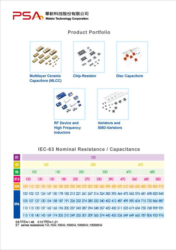
INDEX. How to Order Chip Resistors Selection Guide... 2~ Chip Resistors Array : Convex Termination...
|
|
|
- Imogene Lawson
- 6 years ago
- Views:
Transcription
1
2
3 INDEX Subject Page How to Order Chip Resistors Selection Guide... 2~ Chip Resistors Array : Convex ermination Chip Resistors Array : Concave ermination Special Chip Resistors est and Requirements
4 HO O ORDER R 06 X 1000 F Size code Functional code olerance Packaging code 25 : 2512 (6432) X : 5%: 1ohm ~ 10Mohm F : +/- 1% P : 4 reel taping 20 : 2010 (5025) 1%: 10ohm ~ 1Mohm J : +/- 5% : 7 reel taping 18 : 1218 (3248) : 1%: <10ohm ; >1Mohm P : Jumper A : 7 reel taping 15Kpcs 12 : 1206 (3216) F : 1% for <10ohm ; >1Mohm Q : 10 reel taping 10 : 1210 (3225) (C100ppm) G : 13 reel taping 08 : 0805 (2012) R : mm pitch 06 : 0603 (1608) taping 04 : 0402 (1005) B : Bulk 02 : 0201 (0603) K : Bulkcase 01: 0100 (0402) ype code R: General 1~10MR MR: Automotive SR: Anti-Sulfuration Resistance E24(J tol.) : 2 significant digits followd by No. of zeros and a blank e.g. : 3ohm=3R0_ 10ohm=100_ 220ohm=221_ 56Kohm=563_ ( _ means blank) E24,E96(F tol.) : 3 significant digits followed by No. of zeros e.g.: 3ohm=3R00 10ohm=10R0 220ohm= kohm = 5602 ermination code = Sn base (ead free) (total) 25 M R002 F Size code Functional code Resistance olerance Packaging code 25 : 2512 (6432) X : hick film low ohm R followed by 3 F : +/- 1% P : 4 reel taping 20 : 2010 (5025) M : Metal low ohm significant digits G : +/- 2% : 7 reel taping 18 : 1218 (3248) N : Metal low ohm, high power e.g. : 0.1ohm=R100 J : +/- 5% Q : 10 reel taping 12 : 1206 (3216) : hick film low CR 0.033ohm=R033 G : 13 reel taping 10 : 1210 (3225) P : hick film low CR high 0.56ohm=R560 R : mm pitch 08 : 0805 (2012) power ( 2512 size=2 watt, taping 06 : 0603 (1608) 2010 size=1 watt, B : Bulk 04 : 0402 (1005) 1210 size=0.5 watt, K : Bulkcase 1206 size=0.5 watt, ype code : R< 1ohm M: R< 1ohm Automotive S: R< 1ohm Anti-sulfuration ermination code = Sn base (ead free) G = Au base S = Ag base F 04 H 1001 B Size code Packaging code 25 : 2512 (6432) P : 4 reel taping 20 : 2010 (5025) : 7 reel taping 18 : 1218 (3248) Q : 10 reel taping 12 : 1206 (3216) G : 13 reel taping 10 : 1210 (3225) R : mm pitch 08 : 0805 (2012) taping 06 : 0603 (1608) B : Bulk 04 : 0402 (1005) K : Bulkcase ype code F: Special function MF: Special function Automotive SF: Special function Antisulfuration ype code A: Array MA: Array Automotive SA: Array Anti-sulfuration Functional code G : High ohmic (>10Mohm) H : hick film, Precision tolerance<1% K : hick film, CR50ppm M : rimmable P : High power S : Surge : hin film, CR50ppm U : hin film, CR25ppm Q: hin film C50, power R: hin film C25, power : hin film C10 F: hin film C15 V : High voltage X : Special resistance Y : E24/E96 resistance with special termination (non Resistance E24(J tol.) : 2 significant digits followd by No. of zeros and a blank e.g. : 3ohm=3R0_ 10ohm=100_ 220ohm=221_ 56Kohm=563_ ( _ means blank) E24,E96(F tol.) : 3 significant digits followd by No. of zeros e.g.: 3ohm=3R00 10ohm=10R0 220ohm= kohm = 5602 olerance A : ±0.05% B : +/- 0.1% C : +/- 0.25% D : +/- 0.5% F : +/- 1% G : +/- 2% J : +/- 5% K : +/- 10% : +/- 15% M : +/- 20% P : Jumper X : 0/-30% Y : 0/-20% Z : 0/-10% Remark: 1. Detail product part number, functional code, tolerance combination,...please refer to specific data sheet. 2. Example: ( _ means blank) Chip-R 0805 size, 4.3ohm, 5% Normal type, Sn termination, 5000pcs taped in reel: R08X4R3_J standard packing q ty is 3Kpcs in 10 reel and packing code is code ermination code = Sn base (ead free) G = Au base S = Ag base A 04 Y 103_ J Size code 06 : 0603 (1608) 04 : 0402 (1005) ype code : Network Resistors Functional code X : *4, convex Y : *2, convex : *8, convex : *4, concave U : *2, concave P : *3, convex (Attenuator) Resistance E24(J tol.) : 2 significant digits followd by No. of zeros and a blank e.g. : 3ohm=3R0_ 10ohm=100_ 220ohm=221_ 56Kohm=563_ ( _ means blank) E24,E96(F tol.) : 3 significant digits followd by No. of zeros olerance F : +/- 1% J : +/- 5% P : Jumper Packaging code : 7 reel taping Q : 10 reel taping G : 13 reel taping B : Bulk K : Bulkcase ermination code = Sn base (ead free) 04 X 103_ J Size code Functional code olerance Packaging code 04 : total package X : *8, convex J : +/- 5% : 7 reel taping size 1206 B : Bulk (3216) Resistance E24(J tol.) : 2 significant digits followd by No. of zeros and a blank e.g. : 3ohm=3R0_ 10ohm=100_ 220ohm=221_ 56Kohm=563_ ( _ means blank) E24,E96(F tol.) : 3 significant digits followd by No. of zeros ermination code = Sn base (ead free) 21
5 Chip Resistors Selection Guide Series Size Rated Power olerance Resistance R02X 0201 (0603) 1/20 R04X 0402 (1005) 1/16 R06X 0603 (1608) 1/10 R08X 0805 (2012) 1/8 R12X 1206 (3216) 1/4 R10X 1210 (3225) 1/3 R18X 1218 (3248) 1 R20X 2010 (5025) 1/2 R25X 2512 (6432) ±1% 200 ±5% 100 ±1% 200* ±5% 100 ±1% 200 ±5% 100 ±1% 200 ±5% 100 ±1% 200 ±5% 100 ±1% 200 ±5% 100 ±1% 200 ±5% 100 ±1% 200 ±5% 100 ±1% 200 ±5% Remark : 1. Detailed resistance v.s. CR and ordering code please refer to specific specifications. 2. Jumper resistor is not designed for fusing applications, designers shall apply dedicate fusible resistors or standard fuse in application circuits. Series Size Rated Power olerance Resistance 25X 2512 (6432) 1 18X 1218 (3248) 1 20X 2010 (5025) 1/2 10X 1210 (3225) 1/ X 1206 (3216) 1/4 08X 0805 (2012) 1/8 06X 0603 (1608) 1/10 04X 0402 (1005) 1/16 ±1% ±5% ±1% ±5% ±1% ±5% ±1% ±5% ±1% ±5% ±1% ±5% ±1% ±5% ±1% ±5% Remark : 1. ** Detail resistance v.s. CR please refer to detailed specification. 2. Resistance value will be changed by soldering condition and design of soldering pad, please design products in consideration of this change of resistance value. Series Size Rated Power olerance Resistance 25P 2512 (6432) 2 < 0.100ohm: 150ppm ±1% ±5% 20P 2010 (5025) 1 < 0.100ohm: 150ppm ±1% 0.100ohm: 100ppm ±5% 10P 1210 (3225) 1/2 < 0.100ohm: 500ppm ±1% 0.100ohm: 200ppm ±5% 12P 1206 (3216) 1/2 < 0.100ohm: 200ppm ±1% 0.100ohm: 100ppm ±5% 08P 0805 (2012) 1/3 < 0.100ohm: 200ppm ±1% 0.100ohm: 150ppm ±5% 06P 0603 (1608) 1/4 < 0.100ohm: 250ppm ±1% 0.100ohm: 200ppm ±5% 04P 0402 (1005) 1/8 < 0.470ohm: 300ppm ±1% 0.470ohm: 200ppm ±5% Chip Attenuator Series Size ype ermination ype olerance Attenuation Impedance A04P 0402x2 (1005x2) 4p3R, II type Convex ±0.2db ~ 1dB 1dB ~ 10dB 50 32
6 Chip Resistors Array 43 Series Size Rated Power olerance Resistance 25M 2512 (6432) 1 ±1%, ±5% 25N 2512 (6432) 2 ±1%, ±5% 25Q 2512 (6432) 1 ±1%, ±5% 25R 2512 (6432) 2 ±1%, ±5% 20N 2010 (5025) 1 ±1%, ±5% 12N 1206 ( 3216) 1 ±1%, ±5% 12R 1206 ( 3216) 1 ±1%, ±5% 06R 0603 ( 1608) 1/3 ±1%, ±5% Remark : Resistance value will be changed by soldering condition and design of soldering pad, please design products in consideration of this change of resistance value. * Resistance range in detail specified in specification For detailed resistance range, please refer to specification specified Series Size Rated Power ermination ype olerance Resistance A06X 1206 (0603x4) 1/10 Convex ±1%, ±5% A (0603x4) 1/10 Concave ±1%, ±5% A06Y 0606 (0603x2) 1/10 Convex ±1%, ±5% A04X 0805 (0402x4) 1/16 Convex ±1%, ±5% A04Y 0404 (0402x2) 1/16 Convex ±1%, ±5% A (0402x4) 1/16 Concave ±1%, ±5% A04U 0404 (0402x2) 1/16 Concave ±1%, ±5% A (0602x8) 1/16 Convex ±1%, ±5% Series Size Rated Power ermination ype olerance Resistance 04X 1206 (10P8R) 1/16 Convex ±5% ype Series Size Rated Power olerance Resistance High Power Automotive & Anti-Sulfuration Surge High Voltage High Precision F25P 2512 (6432) 2 F20P 2010 (5025) 1 F10P 1210 (3225) 1/2 F12P 1206 (3216) 1/2 ±1%, ±5% F08P 0805 (2012) 1/4 F06P 0603 (1608) 1/8 F04P 0402 (1005) 1/10 MR12X/SR12X 1206 (3216) 1/4 MR08X/SR08X 0805 (2012) 1/8 MR06X/SR06X 0603 (1608) 1/10 ±1%, ±5% MR04X/SR04X 0402 (1005) 1/16 F25S 2512 (6432) 1 F20S 2010 (5025) 1/2 ±5%, ±10%, ±20% F12S 1206 (3216) 1/4 F25V 2512 (6432) 1 F20V 2010 (5025) 1/2 ±1%, ±5% F12V 1206 (3216) 1/4 F12H 1206 (3216) 1/4 F08H 0805 (2012) 1/8 ±0.1% F06H 0603 (1608) 1/10 ±0.5% F04H 0402 (1005) 1/16 F (3216) 1/8 F08 1/10 ±0.05% 0805 (2012) ±0.10% F08Q 1/8 ±0.25% F06 1/ (1608) ±0.50% F06Q 1/10 ±1.0% F (1005) 1/16 F12U 1206 (3216) 1/8 F08U 1/10 ±0.05% 0805 (2012) ±0.10% F08R 1/8 ±0.25% F06U 1/ (1608) ±0.50% F06R 1/10 ±1.0% F04U 0402 (1005) 1/16 F08F 0805 (2012) 1/10 ±0.05% F06F 0603 (1608) 1/16 ±0.10% F (2012) 1/10 ±0.05% F (1608) 1/16 ±0.10%
.")


 2010 (5025) 1218(3248) 1210 (3225) 1206 (3216) 0805 (2012) 0603 (1608) 0402 (1005) 0201 (0603) Resistance Range ±5% olerance (E24)")
7 Feature 1. High reliability and stability 2. Reduced size of final equipment 3. ower assembly costs 4. Higher component and equipment reliability 5. RoHS compliant and lead free products Description he resistors are constructed in a high grade ceramic body (aluminum oxide). Internal metal electrodes are added at each end and connected by a resistive paste that is applied to the top surface of the substrate. he composition of the paste is adjusted to give the approximate resistance required and the value is trimmed to within tolerance by laser cutting of this resistive layer. Application 1. Consumer electrical equipment, PDA, Digital Camcoder, EDP, Computer application 3. Mobile phone, elecom 4. Power supply, Battery charger, DC-DC power converter 5. Digital meter 6. Automotives aser trimmed Resistive element Primary ayer Protective ayer Marking he resistive layer is covered with a protective coat. Finally, the two external end terminations are added. For ease of soldering the outer layer of these end terminations is in solder(pb free) alloy. ermination Alumina substrate Series No. R25X R20X R18X R10X R12X R08X R06X R04X R02X Size Code 2512 (6432) 2010 (5025) 1218(3248) 1210 (3225) 1206 (3216) 0805 (2012) 0603 (1608) 0402 (1005) 0201 (0603) Resistance Range ±5% olerance (E24) ±1% olerance (E24+E96) ± 200 ± 300 Max. amb=70ºc 1.0 att 1/2 att 1.0 att 1/3 att 1/4 att 1/8 att 1/10 att 1/16 att 1/20 att Max. Operation Voltage (DC or RMS) 250V 200V 200V 200V 200V 150V 50V 50V 25V Climatic category (IEC 60068) 55/155/56 55/125/56 Basic Specification JIS C / IEC Note : 1. his is the maximum voltage that may be continuously supplied to the resistor element, see IEC publication Max. Operation Voltage : So called RCV (Rated Continuous orking Voltage) is determined by RCV= Rater Power x Resistance Value or Max. RCV listed above, whichever is lower. 3. Detailed CR please refer to specific specification. Physical Dimensions Size 2512(6432) 2010(5025) 1218(3248) 1210(3225) 1206(3216) 0805(2012) 0603(1608) 0402(1005) 0201(0603) 6.40 ± ± ± ± ± ± ± ± ± ± ± ± ± ± ± ± ± ± ± ± ± ± ± ± ± ± ± 0.03 b 0.90 ± ± ± ± ± ± ± ± ± 0.05 t 0.65 ± ± ± ± ± ± ± ± ± 0.05 b t End termination Resistive ayer Ceramic Substrate Power Deration Curve For resistors operated in ambient temperature over 70ºC, power rating should be derated in accordance with the following figures Rated Power (%) Rated Power (%) Ambient emperature (ºC) For Climatic category (IEC 60068) 55/155/ Ambient emperature (ºC) For Climatic category (IEC 60068) 55/125/56 (for 0201 type) 54

 passed on it. he sensing voltage be treated as a signal to trigger the switches (CMOS) ON/OFF duration so that to monitor and/or adjust the output current from inductor.")
8 hick Film ow Ohm/Power ow Ohm Chip Resistors Function For ow Ohm Chip Resistors he low ohmic resistors are used to sense output current in power supply, automotive and engine control management system, and other power sensing application. As shows in figure below, the typical function of low ohmic (power) chip resistor is to be a current sensor (Rsense) to generate the sensing voltage (Vs) for the purpose of feedback control when output current (Io) passed on it. he sensing voltage be treated as a signal to trigger the switches (CMOS) ON/OFF duration so that to monitor and/or adjust the output current from inductor. Simplify to say, Vs = I0 x Rsense. In general case, this feedback voltage is setting around 100mV for considering both on power saving and noise robustness. o sense a 5 ampere average output current, the Rsense resistance value therefore be required as 100mV / 5A = 20 m, the power dissipation will be : P = I 2 x R = 5A 2 x 20m = 0.5 att A low ohmic chip resistor with a power rating of 1.0 watt is recommended on this application in case the power safety margin is taken into account. Series No. 25X 20X 18X 10X 12X 08X 06X 04X Size Code 2512 (6432) 2010 (5025) 1218(3248) 1210(3225) 1206 (3216) 0805 (2012) 0603 (1608) 0402 (1005) Resistance olerance ±5%, ±1% Resistance Range Detailed CR please refer to specific data sheets Max. amb=70ºc 1 att 0.5 att 1 att 1/3 att 1/4 att 1/8 att 1/10 att 1/16 att Max. Operation Voltage (DC or RMS) 250V 200V 200V 200V 200V 100V 50V 50V Climatic category (IEC 60068) 55/155/56 55/125/56 Basic Specification JIS C / IEC Note : 1. his is the maximum voltage that may be continuously supplied to the resistor element, see IEC publication Power derating curve, and detail specification please refer to specific data sheets. 3. Resistance value will be changed by soldering condition and design of soldering pad, please design products in consideration of this change of resistance value. Item General Specification Series No. 25P 20P 12P 08P 06P Size code 2512 (6432) 2010 (5025) 1206 (3216) 0805 (2012) 0603 (1608) Resistance olerance ± 1%,± 5% Resistance Range ±150 ppm/ºc ±150 ppm/ºc ±200 ppm/ºc ±200 ppm/ºc ±250 ppm/ºc ±100 ppm/ºc ±100 ppm/ºc ±100 ppm/ºc ±150 ppm/ºc ±200 ppm/ºc Max. amb=70ºc 2 1 1/2 1/3 1/4 Max. Operation Voltage (DC or RMS) 300V 200V 200V 150V 50V Climatic category (IEC 60068) 55/155/56 Note: 1. his is the maximum voltage that may be continuously supplied to the resistor element, see IEC publication Max. Operation Voltage : So called RCV (Rated Continuous orking Voltage) is determined by RCV = Rated Power x Resistance Value or Max. RCV listed above, whichever is lower loading with total solder-pad and trace size of 300 mm 2 Physical Dimensions 25P 20P 12P 08P 06P 6.30 ± ± ± ± ± ± ± ± ± ± ± ± ± ± ± 0.10 t 0.60 ± ± ± ± ± 0.20 b 1.80 ± ± ± ± ± 0.20 b t End termination Resistive layer Ceramic substrate 65

 2010 (5025) 1206 (3216) Resistance olerance ±5%, ±1% Resistance Range 1~10,12,15,20,25,30,40,50m 1~10,12,15,20,25 m 5,10,15,20m 5,10,15,20,25m Max.")

9 Description he resistors are constructed in a high grade low resistive metal body. he resistive layer is covered with a protective coat and printed a resistance marking code over it. Finally, the two external end terminations are added. For ease of soldering the outer layer of these end terminations is lead free terminations. Resistive element Protective ayer Marking ermination Item General Specification Series No. 25M 25N 20M 20N 12N 12M Size code 2512 (6432) 2010 (5025) 1206 (3216) Resistance olerance ±5%, ±1% Resistance Range 1~10,12,15,20,25,30,40,50m 1~10,12,15,20,25 m 5,10,15,20m 5,10,15,20,25m Max. amb=70ºc 1 2 1/ /2 Max. Operation Voltage (DC or RMS) 250V 250V 200V Max. Overload Voltage (DC or RMS) 500V 500V 400V Climatic category (IEC 60068) 55/155/56 Note : 1. his is the maximum voltage that may be continuously supplied to the resistor element, see IEC publication Power derating curve, and detail specification please refer to specific data sheets. 3. Resistance value will be changed by soldering condition and design of soldering pad, please design products in consideration of this change of resistance value. Physical Dimensions: Symbol ± ± ± ± ± ± ± ± ± 0.25 b t ermination Resistive ayer t 0.65 ± ± ± 0.20 b 0.65 ± ± ± 0.20 Marking Physical Dimensions: Symbol Dimensions 6.40 ± 0.20 b ermination Resistive ayer 3.20 ± 0.20 t 0.60 ± 0.10 t 1.60 ± 0.25 b 1.60 ± 0.25 Marking 76

10 Chip Resistors Array : Convex ermination Feature 1. High reliability and stability 2. Reduced size of final equipment 3. ower assembly cost and higher surface mounted efficiency 4. Higher component and equipment reliability Application 1. Consumer electrical equipment, PDA, Digital Camcoder, EDP, Computer application 3. Mobile phone, elecom 4. DIMM Description and Physical Dimensions he resistors array is constructed in a high grade ceramic body (aluminum oxide). Internal metal electrodes are added at each end and connected by a resistive paste that is applied to the top surface of the substrate. he composition of the paste is adjusted to give the approximate resistance required and the value is trimmed to within tolerance by laser cutting of this resistive layer. he resistive layer is covered with a protective coat. Finally, the two external end terminations are added. For ease of soldering the outer layer of these end terminations is in solder alloy. Marking code description is depended on component size and tolerance. Following figure shown the consctruction of a Chip-R array. Resistor ayer High purity alumina substrate aser trimming Marking Electrod/ermination ing Physical Dimensions ype A06X A04X A06Y A04Y 3.20 ± ± ± ± ± ± ± ± ± ± ± ± 0.10 P 0.80 ± ± ± ± 0.10 A 0.60 ± ± ± ± 0.10 B 0.30 ± ± ± ± 0.15 C 0.40 ± ± G 0.30 ± ± ± ± 0.17 B G A C P Series No. A06X A04X A06Y A04Y Size 0603x4 (1608x4) 0402x4 (1005x4) 0603x2 (1608x2) 0402x2 (1005x2) ermination construction 8p4R, Convex 8p4R, Convex 4p2R, Convex 4p2R, Convex Resistance olerance ±5% (E24 series) Resistance Range 10 1M (E24 series), Jumper (0 ± 200 ppm/ºc ± 200 ppm/ºc ± 300 ppm/ºc Max. amb=70ºc 1/10 att 1/16 att 1/10 att 1/16 att Max. Operation Voltage (DC or RMS) 50V 50V 50V 25V Max. Overload Voltage (DC or RMS) 100V 100V 100V 50V Climatic category (IEC 60068) 55/155/56 55/125/56 Basic Specification JIS C / IEC Circuit Mode: R1=R2(=R3=R4) R1 R2 R3 R4 R1 R2 Note : 1. Power derating curve, and detail specification please refer to specific data sheets. 87


11 A06 Chip Resistors Array 16P8R Description he resistors array is constructed in a high grade ceramic body (aluminum oxide). Internal metal electrodes are added at each end and connected by a resistive paste that is applied to the top surface of the substrate. he composition of the paste is adjusted to give the approximate resistance required and the value is trimmed to within tolerance by laser cutting of this resistive layer. he resistive layer is covered with a protective coat. Finally, the two external end terminations are added. For ease of soldering the outer layer of these end terminations is in (Pb free) solder alloy. Item General Specification Series No. A06 Size 1606 (0602x8) erminaton construction Convex type Resistance olerance ±5% (E24 series) Resistance Range K Jumper (0 ) ± 200 ppm/ºc Max. amb=70ºc 1/16 Max. Operation Voltage (DC or RMS) 50V Max. Overload Voltage (DC or RMS) 100V Climatic category (IEC 60068) 55/125/56 Circuit Mode R1 R2 R3 R4 R5 R6 R7 R8 Note : 1. Power derating curve, and detail specification please refer to specific data sheets. Physical Dimensions Symbol Dimensions 4.00 ± ± 0.15 B G 0.45 ± 0.10 B 0.30 ± 0.20 G 0.30 ± 0.20 H1 D P H2 D 0.20 ± 0.10 P 0.50 ± 0.20 H ± 0.20 H ±


12 Chip Resistors Array : Concave ermination Feature Application 1. High reliability and stability 2. Reduced size of final equipment 3. ower assembly costs and higher surface mounted efficiency 4. Higher component and equipment reliability 5. Strong body and terminations 6. Excellence performance in surface mounting assembly. Description and Physical Dimensions he resistors array is constructed in a high grade ceramic body (aluminum oxide). Internal metal electrodes are added at each end and connected by a resistive paste that is applied to the top surface of the substrate. he composition of the paste is adjusted to give the approximate resistance required and the value is trimmed to within tolerance by laser cutting of this resistive layer. he resistive layer is covered with a protective coat. Finally, the two external end terminations are added. For ease of soldering the outer layer of these end terminations is in solder alloy. Marking code description is depended on component size and tolerance. Following figure shown the construction of a Chip-R array. ltem 1. Consumer electrical equipment, PDA, Digital Camcoder, EDP, Computer application 3. Mobile phone, elecom 4. DIMM Resistive ayer General Specification Protect coat Electrod/ermination Electrod/ermination aser trimming Series No. A06 A04 Size 0603x4 (1608x4) 0402x4 (1005x4) erminaton construction Concave type Concave type Resistance olerance ±5% (E24 series) ±5% (E24 series) Resistance Range 10 1M, Jumper (0 10 1M, Jumper (0 ± 200 ppm/ºc ± 300 ppm/ºc Max. amb=70ºc 1/10 1/16 Max. Operation Voltage (DC or RMS) 50V 25V Max. Overload Voltage 100V 50V Climatic category (IEC 60068) 55/125/56 55/125/56 Marking High purity alumina substrate Protect coat Circuit Mode R1 R2 R3 R4 B Note : 1. Power derating curve, and detail specification please refer to specific data sheets. 2. ead Free (Pb free) products are available upon customer s request. A P C G R1=R2=R3=R /-0.10 mm 2.00 ± 0.10mm /-0.10 mm 1.00 ± 0.10mm 0.60 ± 0.20 mm 0.40 ± 0.10 mm P 0.80 ± 0.10 mm 0.50 ± 0.05mm A 0.60 ± 0.15 mm 0.35 ± 0.05 mm B 0.35 ± 0.15 mm 0.20 ± 0.15 mm C 0.50 ± 0.15mm 0.25 ± 0.05 mm G 0.50 ± 0.15 mm 0.25 ± 0.15mm Dimensions Construction Series No. General Specification Series No. A04U Size 0402x2 (1005x2) erminaton construction Concave type Resistance olerance ±5%, ±1% (E24 series) Resistance Range 10 1M, Jumper (0 ± 300 ppm/ºc Max. amb=70ºc 1/16 Max. Operation Voltage (DC or RMS) 25V Max. Overload Voltage 50V Climatic category (IEC 60068) 55/155/56 Note : 1. his is the maximum voltage that may be continuously supplied to the resistor element, see IEC publication Max. Operation Voltage : So called RCV (Rated Continuous orking Voltage) is determined by RCV= Rater Power x Resistance Value or Max. RCV listed above, whichever is lower. A04U 1.00 ± ± ± 0.10 P 0.50 ± 0.05 A 0.35 ± 0.10 Ab 0.35 ± 0.10 B 0.25 ± 0.15 C 0.15 ± 0.10 D 0.25 ±


13 04X Chip Resistors Network Description he resistors array is constructed in a high grade ceramic body (aluminum oxide). Internal metal electrodes are added at each end and connected by a resistive paste that is applied to the top surface of the substrate. he composition of the paste is adjusted to give the approximate resistance required and the value is trimmed to within tolerance by laser cutting of this resistive layer. he resistive layer is covered with a protective coat. Finally, the two external end terminations are added. For ease of soldering the outer layer of these end terminations is in solder (Pb free) alloy. Marking Protective Coat ermination Inner Electrode Resistor aser rimming Item General Specification Series No. 04X Size 0402x8 (1005x8) erminaton construction Convex type Resistance olerance ±5% (E24 series) Resistance Range K ± 200 ppm/ºc Max. amb=70ºc 1/16 att Max. Operation Voltage (DC or RMS) 25V Max. Overload Voltage 50V Climatic category (IEC 60068) 55/155/56 Basic Specification JIS C /IEC Circuit Mode Resistor elements on pin1~pin4, pin6~pin9; R1=R2=R3=R4=R6=R7=R8=R9 pin5 and pin10 common (Grounded). Note : 1. Power derating curve, and detail specification please refer to specific data sheets. 2. ead Free (Pb free) products are available upon customer s request Physical Dimensions 04X 3.30 ± ± ± 0.10 P 0.64 ± 0.05 A 0.50 ± 0.05 B 0.40 ± 0.15 C 0.40 ± 0.15 G 0.40 ± 0.15 B P C G A 10 11

 Frequency range (DC) General")
 Max. 1.")
14 A04P Chip Attenuator A04 P 001 X B Size code ype code Attenuation code olerance Rated voltage ermination Packaging A04: 0402 per element P: convex, type attenuator 001=1dB 002=2dB 003=3dB 004=4dB 005=5dB 006=6dB 010=10dB A: ±0.2dB B: ±0.3dB C: ±0.5dB D: ±1.0dB =7 reel taped = Sn base (lead free) -ype Attenuator (-6dB, 50) for VSR improvement and output frequency level matching on VCO application. Item Series No. Size erminaton construction Attenuation Range Attenuation olerance 1dB ~ 5dB 6dB ~ 10dB Characteristic impedance Rated power at amb=70ºc imiting voltage (DC) Frequency range (DC) General Specification A04P 0402x3 (1005x3) Convex type 1dB, 2dB, 3dB, 4dB, 5dB, 6dB, 7dB, 8dB, 9dB,10dB ±0.3dB ±0.5dB / package 50V Max. 2GHz VSR (Voltage Standing ave Ratio) Max. 1.3 Number of Resistors 3 resistors Number of erminals 4 terminals Climatic category (IEC 60068) 55/125/56 Circuit Configuration 4 3 R1 R2 R2 1 2 Outline of A04P Chip attenuator ing Identification mark Ceramic substrate ermination Physical Dimensions A04P 1.00 ± ± ± 0.10 P 0.65 ± 0.10 A 0.33 ± 0.10 a 0.15 ± 0.10 b 0.25 ± 0.10 a P b Resistor layer Ceramic substrate Inner electrode End termination A 12 11
15 Special Chip Resistors Feature 1. Provided Automotive & Anti-sulfuration resistors (MR/SR series) for Auto & Anti-sulfuration application. 2. Provided otal ead Free resistors (R_R series) to fulfill RoHS environmental regulation. 3. Provided trimmable resistors (FxxM series) for customer special tolerance requirement. 4. Provided high precision tolerance (FxxH/ Fxx/FxxU/Fxx) down to ±0.05% and CR down to 10ppm/ C for voltage sensing application. 5. High reliability and stability 6. Reduced size of final equipment 7. ower assembly costs 8. Higher component and equipment reliability. 9. Special resistance, tolerance are available upon customer s request. MR/SR Series of Automotive & Anti-Sulfuration Chip Resistor Feature Application 1. High reliability and stability ±1% 2. Sulfuration resistant 3. Automotive grade AEC Q-200 compliant % CCD inspection 5. RoHS compliant and lead free 1. Automotive application 2. Consumer electrical equipment 3. EDP, Computer application 4. elecom application Series No. MR12X/SR12X MR08X/SR08X MR06X/SR06X MR04X/SR04X Size code 1206 (3216) 0805 (2012) 0603 (1608) 0402 (1005) Resistance Range Max. amb=70ºc 1/4 1/8 1/10 1/16 Max. Operation Voltage (DC or RMS) 200V 150V 75V 50 Climatic category (IEC 60068) 55/155/56 Remark: *Detail specification please refer to specific data sheets! * MR series can withstand H 2 S 3ppm x 1000 hrs * SR series can withstand H 2 S 1000ppm x 720 hrs R_R Series of otal ead Free Chip Resistors Feature 1. High reliability and stability 2. Reduced size of final equipment 3. ow assembly costs 4. Higher component and equipment reliability 5. RoHS compliant and total lead free Series No. R12_R R08_R R06_R R04_R Size code 1206 (3216) 0805 (2012) 0603 (1608) 0402 (1005) Resistance Range Max. amb=70ºc 1/4 1/8 1/10 1/16 Max. Operation Voltage (DC or RMS) 200V 150V 50V 50 Climatic category (IEC 60068) 55/155/56 Remark: *Detail specification please refer to specific data sheets! 1 st code 2 nd code 3 rd th code 5 th code 6 th th code 10 th code 11 th code 12 th code R C ype code Size code Functional code Marking code (Resistance) olerance code Packaging code ermination code Example R 04 X 1000 F R 13 12
 Description he resistors are constructed on a high-grade ceramic body (aluminum oxide).")

16 FxxM Series of rimmable Chip Resistors Feature 1. High precision, reliability and stability 2. Miniature size to 0603(1608) Description he resistors are constructed on a high-grade ceramic body (aluminum oxide). Internal metal electrodes are added at each and connected by a resistive paste, which is applied to the substrate. he composition of the paste is adjusted to give the approximate resistance required. he resistive layer is converted with a transparent protective coating. Finally the two external end terminations are added. For case of soldering the outer of theses end terminations is in solder (Pb free) alloy. Physical Dimensions F20M F12M F08M F06M 5.00 ± ± ± ± ± ± ± ± ± ± ± ± 0.15 b 0.65 ± ± ± ± 0.20 t 0.60 ± ± ± ± 0.10 Series No. F20M F12M F08M F06M Size code 2010 ( 5025 ) 1206 ( 3216 ) 0805 ( 2012 ) 0603 ( 1608 ) Resistance olerance 0/-10%(Z), 0/-20%(Y) and 0/-30%(X) E24 series Resistance Range 1 10M ± 200 ppm/ºc <10-300~+500 ppm/ºc Max. amb=70ºc 1/2 att 1/4 att 1/8 att 1/10 att Max. Operation Voltage (DC or RMS) 200V 200V 100V 50V Climatic category (IEC 60068) 55/125/56 Basic Specification JIS C / IEC Application 1. Automotive application 2. Consumer electrical equipment 3. EDP, Computer application 4. elecom application End termination Resistive layer Ceramic substrate b t End termination Resistive layer Ceramic substrate Please refer to specific data sheet. FxxV Series of High Voltage Chip Resistors Feature 1. Special material and design for high working voltage required Suitable for lead free soldering. Application 1. Power supply 2. Automotive industry 3. Measurement instrument 4. Back light inverter 5. Medical or Military equipment Item General Specification Series No. F25V F20V F12V Size code 2512 (6432) 2010 (5025) 1206 (3216) Resistance olerance ± 5% ; ± 1% Resistance Range 100 K 10 M ± 200 ppm/ºc Max. amb=70ºc 1 1/2 1/4 Max. Operation Voltage (DC or RMS) 2000V 1500V 800V Max. Overload Voltage (DC or RMS) 4000V 3000V 1600V Climatic category (IEC 60068) 55/155/56 Note: 1. his is the maximum voltage that may be continuously supplied to the resistor element, see IEC publication Max. Operation Voltage : So called RCV (Rated Continuous orking Voltage) is determined by RCV = Rated Power x Resistance Value or Max. RCV listed above, whichever is lower. End termination b Physical Dimensions Symbol F25V F20V F12V 6.30 ± ± ± ± ± ± ± ± ± 0.10 t 0.60 ± ± ± 0.25 b 0.90 ± ± ± 0.25 t Resistive layer Ceramic substrate 14 13


17 FxxP Series of High Power Chip Resistors Feature 1. High power rating and compact size 2. High reliability and stability ead free product is upon customer requested. Note: 1. his is the maximum voltage that may be continuously supplied to the resistor element, see IEC publication Max. Operation Voltage : So called RCV (Rated Continuous orking Voltage) is determined by RCV = Rated Power x Resistance Value or Max. RCV listed above, whichever is lower loading with total solder-pad and trace size of 300 mm maximum resistance Rmax < 15m and rated current < 4Amp Physical Dimensions t b Item F25P 6.30 ± ± ± ± ± 0.25 F20P 5.00 ± ± ± ± ± 0.25 F12P 3.10 ± ± ± ± ± 0.25 F08P 2.00 ± ± ± ± ± 0.20 Application 1. Power supply 2. PDA 3. Digital meter 4. Computer 5. Automotives 6. Battery charger General Specification 7. DC-DC power converter Series No. F25P F20P F12P F08P F06P Size code 2512 (6432) 2010 (5025) 1206 (3216) 0805 (2012) 0603 (1608) Resistance olerance ± 1%,± 5% ±1% ±5% ±1% ±5% Resistance Range 0 1 ~ 1 M ± 100 ppm/ºc Max. amb=70ºc 2 1 1/2 1/4 1/8 Max. Operation Voltage (DC or RMS) 300V 200V 200V 150V 50V Climatic category (IEC 60068) 55/155/56 F06P 1.60 ± ± ± ± ± 0.20 b t End termination Resistive layer Ceramic substrate FxxS Series of Surge Chip Resistors Feature 1. Power rating and compact size 2. High reliability and stability Surge protection Item General Specification Series No. F25S F20S F12S Size code 2512 (6432) 2010 (5025) 1206 (3216) Resistance olerance ±5%, ±10%, ±20%, (E24) Resistance Range 10 1M ± 100 ppm/ºc Max. amb=70ºc 1 1/2 1/4 Max. Operation Voltage (DC or RMS) 200V 200V 200V Max. Overload Voltage (DC or RMS) 400V 400V 400V Climatic category (IEC 60068) 55/125/56 Note: 1. his is the maximum voltage that may be continuously supplied to the resistor element, see IEC publication Max. Operation Voltage : So called RCV (Rated Continuous orking Voltage) is determined by RCV = Rated Power x Resistance Value or Max. RCV listed above, whichever is lower. Physical Dimensions F25S F20S F12S 6.30 ± ± ± ± ± ± ± ± ± 0.10 t 0.60 ± ± ± 0.25 b 0.60 ± ± ± 0.25 Application 1. Power supply 2. Measurement instrument 3. Automotive industry 4. Medical or Military equipment b t End termination Resistive layer Ceramic substrate 15 14
18 High Precision Chip Resistors Series No. F12H F08H F06H F04H Size code 1206 ( 3216 ) 0805 ( 2012 ) 0603 ( 1608 ) 0402 ( 1005 ) Resistance olerance ±0.5%, ±0.1% Resistance Range 10 1M E24 series ) 10M 1M ± 100 ppm/ºc ± 200 ppm/ºc Max. amb=70ºc 1/4 att 1/8 att 1/10 att 1/16 att Max. Operation Voltage (DC or RMS) 200V 100V 50V 50V Climatic category (IEC 60068) 55/155/56 Basic Specification JIS C / IEC (Detail specification please refer to specific data sheets) Series No. F12 F08 F06 F04 F08Q F06Q Size code 1206 ( 3216 ) 0805 ( 2012 ) 0603 ( 1608 ) 0402 ( 1005 ) 0805 ( 2012 ) 0603 ( 1608 ) Resistance olerance ±0.5%, ±0.1% ± 50 ppm/ºc Max. amb=70ºc 1/8 att 1/10 att 1/16 att 1/16 att 1/8 att 1/10 att Max. Operation Voltage (DC or RMS) 200V 100V 50V 50V 150V 50V Climatic category (IEC 60068) 55/125/56 Basic Specification JIS C / IEC (Detail specification please refer to specific data sheets) Series No. F12U F08U F06U F04U F08R F06R Size code 1206 ( 3216 ) 0805 ( 2012 ) 0603 ( 1608 ) 0402 ( 1005 ) 0805 ( 2012 ) 0603 ( 1608 ) Resistance olerance ±0.5%, ±0.1%, ±0.05% ± 25 ppm/ºc Max. amb=70ºc 1/8 att 1/10 att 1/16 att 1/16 att 1/8 att 1/10 att Max. Operation Voltage (DC or RMS) 200V 100V 50V 50V 150V 50V Climatic category (IEC 60068) 55/125/56 Basic Specification JIS C / IEC (Detail specification please refer to specific data sheets) Series No. F12F* F08F F06F F04F* Size code 1206 ( 3216 ) 0805 ( 2012 ) 0603 ( 1608 ) 0402 ( 1005 ) Resistance olerance ±0.5%, ±0.1%, ±0.05% Max. amb=70ºc 1/8 att 1/10 att 1/16 att 1/16 att Max. Operation Voltage (DC or RMS) 200V 100V 50V 50V Climatic category (IEC 60068) 55/125/56 Basic Specification JIS C / IEC (Detail specification please refer to specific data sheets) * Sample is available upon request Series No. F12* F08 F06 F04* Size code 1206 ( 3216 ) 0805 ( 2012 ) 0603 ( 1608 ) 0402 ( 1005 ) Resistance olerance ±0.5%, ±0.1%, ±0.05% Max. amb=70ºc 1/8 att 1/10 att 1/16 att 1/16 att Max. Operation Voltage(DC or RMS) 200V 100V 50V 50V Climatic category (IEC 60068) 55/125/56 Basic Specification JIS C / IEC (Detail specification please refer to specific data sheets) * Sample is available upon request 16 15
19 est and Requirements est Electrical Characteristics Clause 4.8 Resistance to soldering heat (R.S.H) JISC5201-1:1998 Clause 4.18 Solderability Clause 4.17 emperature cycling Clause 4.19 High emperature Exposure MI-SD-202 method 108 Bending strength Clause 4.33 Adhesion JISC5201-1: 19 Clause 4.32 Short ime Overload (SO) Clause 4.13 oad life in Humidity Clause 4.24 oad life (endurance) Clause 4.25 Insulation Resistance Clause 4.6 Dielectric ithstand Voltage Clause 4.7 Procedure / est Method - DC resistance values measurement - emperature Coefficient of Resistance (.C.R) Natural resistance change per change in degree centigrade. R2 - R1 (ppm/ C) t1 : 20 C+5 C-1 C R1 (t2 - t1) X106 R1 : Resistance at reference temperature (20 C+5 C/-1 C) R2 : Resistance at test temperature (-55 C or +155 C) Un-mounted chips completely immersed for 10±1second in a SAC solder bath at 260ºC±5ºC Un-mounted chips completely immersed for 2±0.5 second in a SAC solder bath at 235ºC±5ºC 30 minutes at -55ºC±3ºC, 2~3 minutes at 20 C+5 C-1 C, 30 minutes at +155ºC±3ºC, 2~3 minutes at 20 C+5 C-1 C, total 5 continuous cycles /-0 hours; without load in a temperature chamber controlled 155±3ºC Resistors mounted on a 90mm glass epoxy resin PCB(FR4), bending once 3mm for 10sec, 5mm for R04 Pressurizing force: 5N, est time: 10±1sec. 2.5 times RCV or max. overload voltage, for 5seconds /-0 hours, loaded with RCV or Vmax in humidity chamber controller at 40ºC±2ºC and 90~95% relative humidity, 1.5hours on and 0.5 hours off /-0 hours, loaded with RCV or Vmax in chamber controller 70±2ºC, 1.5 hours on and 0.5 hours off Apply the maximum overload voltage (DC) for 1minute Apply the maximum overload voltage (AC) for 1 minute Requirements Resistor ithin the specified tolerance Refer to QUICK REFERENCE DAA no visible damage 95% coverage min., good tinning and no visible damage no visible damage No visible damage visual damaged No remarkable damage or removal of the terminations No visible damage No visible damage No visible damage No breakdown or flashover 17 16
20 est Electrical Characteristics Clause 4.8 Short ime Overload (SO) Clause 4.13 Solderability Clause 4.17 Resistance to soldering heat (R.S.H) JISC5201-1:1998 Clause 4.18 emperature cycling Clause 4.19 oad life (endurance) Clause 4.25 oad life in Humidity Clause 4.24 Bending strength Clause 4.33 Adhesion JISC5201-1: 19 Clause 4.32 Insulation Resistance Clause 4.6 Dielectric ithstand Voltage Clause 4.7 Procedure / est Method - DC resistance values measurement - emperature Coefficient of Resistance (.C.R) Natural resistance change per change in degree centigrade. R2 - R1 (ppm/ C) t1 : 20 C+5 C-1 C R1 (t2 - t1) X106 R1 : Resistance at reference temperature (20 C+5 C/-1 C) R2 : Resistance at test temperature (-55 C or +155 C) 2.5 times RCV or max. overload voltage, for 5seconds Un-mounted chips completely immersed for 2±0.5 second in a SAC solder bath at 235ºC±5ºC Un-mounted chips completely immersed for 10±1second in a SAC solder bath at 260ºC±5ºC 30 minutes at -55ºC±3ºC, 2~3 minutes at 20 C+5 C-1 C, 30 minutes at +155ºC±3ºC, 2~3 minutes at 20 C+5 C-1 C, total 5 continuous cycles /-0 hours, loaded with RCV or Vmax in chamber controller 70±2ºC, 1.5 hours on and 0.5 hours off /-0 hours, loaded with RCV or Vmax in humidity chamber controller at 40ºC±2ºC and 90~95% relative humidity, 1.5hours on and 0.5 hours off Resistors mounted on a 90mm glass epoxy resin PCB(FR4), bending once 3mm for 10sec, 5mm for R04 Pressurizing force: 5N, est time: 10±1sec. Apply the maximum overload voltage (DC) for 1minute Apply the maximum overload voltage (AC) for 1 minute Requirements Resistor ithin the specified tolerance Refer to QUICK REFERENCE DAA No visible damage 95% coverage min., good tinning and no visible damage no visible damage no visible damage No remarkable damage or removal of the terminations No breakdown or flashover 17
, A06X, A06 3.60 ± 0.20 2.00 ± 0.20 0805 (2012) 2.40 ± 0.20 1.65 ± 0.20 4.00 ± 0.10 Max.")
 2010 (5025) 1218 (3248) A 6.")
21 Packing on ape and Reel Component Size / Series F E P0 ØD 1206, 0805, 0603, 0402, A06X, A06, A04X, A04Y, A04P, 8.00 ± ± 0.20 A04, A04U, 04X A ± ± 0.05 R02X 8.00 ± ± ± ± 0.10 Ø X-X X P1 P0 ØD A E F Component Size / Series A B P (3216), A06X, A ± ± (2012) 2.40 ± ± ± 0.10 Max (1608) 1.90 ± ± ± (1005) 1.20 ± ± ± ± 0.05 A04X, A ± ± ± 0.05 Max. 0.6 A04Y, A04P, A04U 1.15 ± ± ± ± X / / ± ± 0.05 A / / ± ± 0.05 R02X 0.67 ± ± ± ± 0.05 X B Component Size 2512 (6432) 2010 (5025) 1218 (3248) A 6.90 ± ± ± 0.30 B 3.60 ± ± ± ± 0.30 F 5.50 ± 0.1 E 1.75 ± 0.10 P ± 0.10 P ± ØD Ø Max. 1.2 X-X X X P1 P0 ØD B A E F Reel / ape A B C D 7 reel for 8mm tape 9.0 ± 0.50 Ø178.0 ± 0.2 Ø60.0 ± ± reel for 12mm tape 12.4 ± reel for 8mm tape Ø254.0 ± 2.0 Ø100.0 ± ± ± reel for 12mm tape Ø254.0 ± 2.0 Ø100.0 ± ± ± reel for 8mm tape Ø330.0 ± 2.0 Ø100.0 ± ± ± 0.50 C B A D Component Size / Series Q ty per reel Reel diameter 0603, 0805, ,000 pcs 4 reel 1210, 1206, 0805, 0603, A06X, A06, 04X 5,000 pcs 7 reel 0402, A04X, A04Y, A04P, A04, A04U 10,000 pcs 7 reel 0201, ,000 pcs 7 reel A06X, A06Y 5,000 pcs 7 reel 2512, ,000 pcs 7 reel ,000 pcs 10 reel 1206, 0805, 0603, A06X, A06 10,000 pcs 10 reel 0402, A04X, A04Y 20,000 pcs 10 reel 2010, ,000 pcs 10 reel ,000 pcs 13 reel A04X, A04Y 40,000 pcs 13 reel 1206, 0805, 0603, A06X 20,000 pcs 13 reel 2010, ,000 pcs 13 reel 17 18

 ± 0.25 0805 3.40 1.30 1.")
22 Footprint Design E Occupied area D G Solder land/ Solder paste pattern C F A B Solder resist pattern racks or Dummy tracks (for wave soldering only) Size Reflow Soldering A B C D E F G Processing remarks Placement Accuracy ± ± ± ± 0.25 IR or hot plate soldering ± ± ± ± 0.25 Size ave Soldering A B C D E F G Processing number & Dimensions of dummy tracks Placement Accuracy x (0.15 x 0.80) ± x (0.20 x 1.30) ± x (0.25 x 1.70) ± x (0.25 x 4.80) ± x (0.75 x 2.50) ± x (1.00 x 3.20) ± 0.25 Symbol 0603*4 array 0402*4 array A04Y, A04P A06 A / / ± / B 0.45 ± ± / / D 0.80 ± ± ± / P F 3.10 ± / / ± 0.40 P A D B F Symbol 04X ± ± 0.05 H ± 0.10 P ± 0.05 P ± 0.05 A 3.20 ± 0.10 F / H1 H2 F P2 P1 A 19


23 Storage and Handling Conditions: 1. Products are recommended to be used up within one year. Check solderability in case shelf life extension is needed. 2. o store products with following condition: emperature : 5 to 40 C Humidity : 20 to 70% relative humidity 3. Caution: a. Don t store products in a corrosive environment such as sulfide, chloride gas, or acid. It may cause oxidization of electrode, which easily be resulted in poor soldering. b. o store products on the shelf and avoid exposure to moisture. c. Don t expose products to excessive shock, vibration, direct sunlight and so on. Figure. IR reflow soldering profile for SM process with SnAgCu series solder paste. Figure. IR reflow soldering profile for SM process with eutectic SnPb solder paste. ernperoture (Deg.C.) ernperoture (Deg.C.) yplcally vatues Process limits ime <100 sec otal contact time yplcally <5 300degc, 350degc, as short as possibla ime Figure. ave soldering Figure. Manual soldering (soldering gun) 20
24 PAN & MEMO
25

26
High Power Low Ohm Chip Resistors. Size W, W, /2W
 WW25P, WW20P, WW12P ±1%, ±5% 47mΩ~976mΩ High Power Low Ohm Chip Resistors Size 2512 2W, 2010 1W, 1206 1/2W *Contents in this sheet are subject to change without prior notice. Page 1 of 7 ASC_WW25P-20P-12P_V08
High Power Chip Resistors Size W, W, /2W
 WF25P, WF20P, WF12P ±1%, ±5% 0Ω,1Ω~1MΩ High Power Chip Resistors Size 2512 2W, 2010 1W, 1206 1/2W Customer : Approval No : Issue Date : Customer Approval : Page 1 of 7 WF25P, WF20P, WF12P, Ver.8 Jul.2010
WA04X, WA06X ±1%, ±5%, Convex Type General purpose chip resistors array
 WA04X, WA06X ±1%, ±5%, Convex Type General purpose chip resistors array Size 0402x4, 0603x4 (8p4R) (Automotive ) Page 1 of 8 ASC_WAxxX_J_V05 May.2011 FEATURE 1. Small size and light weight 2. Reduced size
1 7 ASC_WF06A_V01 NOV
 WF06A 1 ~ 1Mohm ±5%, ±1% High Power Chip Resistors Size 0603 1/4W *Contents in this sheet are subject to change without prior notice. Page 1 of 7 ASC_WF06A_V01 NOV - 2015 FEATURE 1. Small size and light
WF08P, WF06P. High Power Chip Resistors Size /4W ; /8W. Customer : Approval No : Issue Date : Customer Approval :
 WF08P, WF06P ±1%, ±5% 0Ω, 1Ω~1MΩ High Power Chip Resistors Size 0805 1/4W ; 0603 1/8W Customer : Approval No : Issue Date : Customer Approval : Page 1 of 7 WF08P;WF06P Version 04 Jul.-2009 FEATURE 1. Small
SPECIFICATION SHEET. ±1%, ±5%, Convex Type General purpose chip resistors array
 SPECIFICATION SHEET CNA24, CNA34 ±1%, ±5%, Convex Type General purpose chip resistors array Size 0402x4, 0603x4 (8p4R) ( Automotive & Anti-sulfur ) All data in this sheet are subject to change, modify
WW12W ±1%, ±5% Size W. Thick Film High Power Low Ohm Chip Resistors. Approval sheet
 ±1%, ±5% Thick Film High Power Low Ohm Chip Resistors Size 1206 1W *Contents in this sheet are subject to change without prior notice. Page 1 of 6 ASC 1W TC200_V01 DEC - 2015 FEATURE 1. High power rating
WF25S WF20S WF12S ±5% 20% Power Surge Chip Resistors Size 2512, 2010, Customer : Approval No : Issue Date : Customer Approval :
 WF25S WF20S WF12S ±5% 5%, ±10 10%, ±20 20% Power Surge Chip Resistors Size 2512, 2010, 1206 Customer : Approval No : Issue Date : Customer Approval : Page 1 of 7 WF25S WF20S WF12S Ver.4 Sep.-2008 FEATURE
WA04X ±5%, Convex Type General purpose chip resistors array Size 0402x4
 WA04X ±5%, Convex Type General purpose chip resistors array Size 0402x4 Customer : Approval No : Issue Date : Customer Approval : Page 1 of 7 WA04X Version 20 Sep.-2008 FEATURE 1. Small size and light
WA04X ±5%, Convex Type General purpose chip resistors array Size 0402x4
 WA04X ±5%, Convex Type General purpose chip resistors array Size 0402x4 Customer : Approval No : Issue Date : Customer Approval : Page 1 of 8 WA04X Version 15 Sept.-2004 FEATURE 1. Small size and light
WT04X ±5%, Convex Type 10p8R Chip resistors network Size 1206
 WT04X ±5%, Convex Type 10p8R Chip resistors network Size 1206 Customer : Approval No : Issue Date : Customer Approval : Page 1 of 7 WT04X Ver.13 Sep.-2008 FEATURE 1. Small size and light weight 2. Reduced
WR18X(W), WR20X(W), WR25X(W) ±1%, ±5% Power chip resistors Size 1218,2010,2512
, WR20X(W), WR25X(W) ±1%, ±5% Power chip resistors Size 1218,2010,2512") WR18X(W), WR20X(W), WR25X(W) ±1%, ±5% Power chip resistors Size 1218,2010,2512 Customer : Approval No : Issue Date : Customer Approval : Page 1 of 7 WR18-20-25X(W) Ver.13 Oct.-2010 FEATURE 1. High power
WR18X(W), WR20X(W), WR25X(W) ±1%, ±5% Power chip resistors Size 1218,2010,2512 Customer : Approval No : Issue Date : Customer Approval : Page 1 of 7 WR18-20-25X(W) Ver.13 Oct.-2010 FEATURE 1. High power
MA04X, MA06X ±1%, ±5%, Convex Type General purpose chip resistors array
 MA04X, MA06X ±1%, ±5%, Convex Type General purpose chip resistors array Size 0402x4, 0603x4 (8p4R) ( Automotive & Anti-sulfur ) Page 1 of 8 MA04/ 06_V03 Apr.2010 FEATURE 1. High reliability and stability
WF10H ±0.1%, ±0.5% High Precision chip resistors Size 1210
 WF10H ±0.1%, ±0.5% High Precision chip resistors Size 1210 *Contents in this sheet are subject to change without prior notice. Page 1 of 7 ASC_WF10H_V01 Jan.2010 FEATURE 1. High reliability and stability
WF20M / WF12M / WF08M / WF06M 0/-20% and 0/-30% Trimmable chip resistors
 WF20M / WF12M / WF08M / WF06M 0/-20% and 0/-30% Trimmable chip resistors Size 2010, 1206, 0805, 0603 Page 1 of 7 WFxxM Trimmable_V11 Apr.2010 FEATURE 1. Reduced size of final equipment 2. Lower assembly
SR20X, SR25X ±1%, ±5% Power chip resistors Size 2010, 2512
 SR20X, SR25X ±1%, ±5% Power chip resistors Size 2010, 2512 ( Automotive & Anti-sulfuration ) Page 1 of 7 SR20-25X_V04 Sep.-2011 FEATURE 1. High reliability and stability ±1% 2. Sulfuration resistant 1000ppm
WR10, WR12, WR08, WR06, WR04 ±1%, ±5% General purpose chip resistors. Size 1210, 1206, 0805, 0603, 0402
 WR10, WR12, WR08, WR06, WR04, General purpose chip resistors Size 1210, 1206, 0805, 0603, 0402 ( Automotive & Anti-sulfuration ) *Contents in this sheet are subject to change without prior notice. Page
WK25S WK20S WK10S WK12S WK08S. Thick Film Power Surge Chip Resistors. Size 2512, 2010, 1210, 1206, 0805
 WK25S WK20S WK10S WK12S WK08S ±5%, ±10%, ±20% Thick Film Power Surge Chip Resistors Size 2512, 2010, 1210, 1206, 0805 *Contents in this sheet are subject to change without prior notice. Page 1 of 7 ASC_WKxxS_V02
WK25S WK20S WK10S WK12S WK08S WK06S. Thick Film Power Surge Chip Resistors. Size 2512, 2010, 1210, 1206, 0805, 0603
 WK25S WK20S WK10S WK12S WK08S WK06S ±5% 5%, ±10 10%, ±20 20% Thick Film Power Surge Chip Resistors Size 2512, 2010, 1210, 1206, 0805, 0603 *Contents in this sheet are subject to change without prior notice.
WR10X ±1%, ±5% General purpose chip resistors Size 1210
 WR10X ±1%, ±5% General purpose chip resistors Size 1210 Customer : Approval No : Issue Date : Customer Approval : Page 1 of 7 WR10X Version 02 Jun.-2005 FEATURE 1. High reliability and stability 2. Reduced
WA04T ±5%, ±1% Concave Type General purpose chip resistors array
 WA04T ±5%, ±1% Concave Type General purpose chip resistors array Size 0402x4 *Contents in this sheet are subject to change without prior notice. Page 1 of 7 ASC_WA04T_Concave_V10 Oct.2010 FEATURE 1. Small
High Power Chip Resistor
 Description: The resistors are constructed in a high grade ceramic body (aluminium oxide). Internal metal electrodes are added at each end and connected by a resistive paste that is applied to the top
Size 1206, 1210, 0805, 0603, 0402 (Anti-Sulfuration )
") SR12, SR10, SR08, SR06, SR04, General purpose chip resistors Size 1206, 1210, 0805, 0603, 0402 (Anti-Sulfuration ) *Contents in this sheet are subject to change without prior notice. Page 1 of 9 ASC_SR_V03
SR12, SR10, SR08, SR06, SR04, General purpose chip resistors Size 1206, 1210, 0805, 0603, 0402 (Anti-Sulfuration ) *Contents in this sheet are subject to change without prior notice. Page 1 of 9 ASC_SR_V03
WW25W, WW20W, WW10W, WW12W, WW08W, WW06W
 WW25W, WW20W, WW10W, WW12W, WW08W, WW06W ±1%, ±5% Thick Film Power Low Ohm Chip Resistors RoHS Exemption free and Lead free Size 2512, 2010, 1210, 1206, 0805, 0603 *Contents in this sheet are subject to
WF12H, WF08H, WF06H, WF04H ±0.1% High precision chip resistors Size 1206, 0805, 0603, 0402
 WF12H, WF08H, WF06H, WF04H ±0.1% High precision chip resistors Size 1206, 0805, 0603, 0402 Customer : Approval No : Issue Date : Customer Approval : Page 1 of 7 WFxxHB ±0.1% Ver.13 Sep.-2008 FEATURE 1.
Thick Film Chip Resistors
 Description: The resistors are constructed in a high grade ceramic body (aluminum oxide). Internal metal electrodes are added at each end and connected by a resistive paste that is applied to the top surface
WR12, WR08, WR06, WR04 ±1%, ±5% General purpose chip resistors. Size 1206, 0805, 0603, ( Automotive )
") WR12, WR08, WR06, WR04 ±1%, ±5% General purpose chip resistors Size 1206, 0805, 0603, 0402 ( Automotive ) Page 1 of 9 WR_J(AUTO)_ V03 Sep.2010 FEATURE 1. Automotive grade AEC Q-200 compliant 2. 100% CCD
WR12, WR08, WR06, WR04 ±1%, ±5% General purpose chip resistors Size 1206, 0805, 0603, 0402 ( Automotive ) Page 1 of 9 WR_J(AUTO)_ V03 Sep.2010 FEATURE 1. Automotive grade AEC Q-200 compliant 2. 100% CCD
WK25S WK20S WK10S WK12S WK08S WK06S. Thick Film Power Surge Chip Resistors AEC Q-200 Qualified Size 2512, 2010, 1210, 1206, 0805, 0603
 WK25S WK20S WK10S WK12S WK08S WK06S ±5% 5%, ±10 10%, ±20 20% Thick Film Power Surge Chip Resistors AEC Q-200 Qualified Size 2512, 2010, 1210, 1206, 0805, 0603 *Contents in this sheet are subject to change
WF12H, WF08H, WF06H, WF04H ±0.5% High precision chip resistors Size 1206, 0805, 0603, 0402
 WF12H, WF08H, WF06H, WF04H ±0.5% High precision chip resistors Size 1206, 0805, 0603, 0402 Customer : Approval No : Issue Date : Customer Approval : Page 1 of 7 WFxxHD ±0.5% Ver.13 March.-2010 FEATURE
WW25X ±1%, ±5% Low ohmic power chip resistors Size 2512
 WW25X ±1%, ±5% Low ohmic power chip resistors Size 2512 Customer : Approval No : Issue Date : Customer Approval : Page 1 of 7 WW25X Version 06 Jul.-2004 FEATURE 1. High power rating and compact size 2.
WR18, WR20, WR25 ±1%, ±5% Power chip resistors Size 1218,2010,2512
 WR18, WR20, WR25 ±1%, ±5% Power chip resistors Size 1218,2010,2512 Customer : Approval No : Issue Date : Customer Approval : Page 1 of 7 WR18, WR20, WR25 Version 3 Oct.-2004 FEATURE 1. High power rating
WA04, WA06 ±1%, ±5%, Convex Type & Concave Type General purpose chip resistors array
 WA04, WA06 ±1%, ±5%, Convex Type & Concave Type General purpose chip resistors array Size 0402x2 (4p2R) Size 0402x4, 0603x4 (8p4R) Size 0602x8 (16p8R) *Contents in this sheet are subject to change without
1 8 WK L_V_AUTO_V01 FEB
 WK12L, WK20L, WK25L 1%, 5% Thick Film Power Chip Resistor Wide Termination RoHS compliant and Halogen free Size 0612, 1020, 1225 Automotive AEC Q200 Compliant ASTM B-809-95 Compliant *Contents in this
Thick Film General purpose chip resistors
 WR02X(W) ±5%, ±1% Thick Film General purpose chip resistors Size 0201 *Contents in this sheet are subject to change without prior notice. Page 1 of 7 ASC_WR02X_V18 MAY - 2016 FEATURE 1. Small size and
WW25X, WW18X, WW12X, WW08X, WW06X ±1%, ±5% Thick Film Current Sensing Chip Resistors Size 2512, 1218, 1206, 0805, 0603 (Automotive)
") WW25X, WW18X, WW12X, WW08X, WW06X ±1%, ±5% Thick Film Current Sensing Chip Resistors Size 2512, 1218, 1206, 0805, 0603 (Automotive) *Contents in this sheet are subject to change without prior notice. Page
WW25X, WW18X, WW12X, WW08X, WW06X ±1%, ±5% Thick Film Current Sensing Chip Resistors Size 2512, 1218, 1206, 0805, 0603 (Automotive) *Contents in this sheet are subject to change without prior notice. Page
WR02X ±5%, ±1% General purpose chip resistors Size 0201
 WR02X ±5%, ±1% General purpose chip resistors Size 0201 Customer : Approval No : Issue Date : Customer Approval : Page 1 of 8 WR02X Version 03 Jul.-2004 FEATURE 1. Small size and light weight 2. High reliability
WF12SR360JTL. Size Surge 5% chip resistors. Customer : Approval No : Issue Date : Customer Approval :
 SPECIFICATION OF SURGE 5% CHIP RESISTOR Ver: 1 Page: 1 of 7 ROHS compliance WF12SR360JTL Surge 5% chip resistors Size 1206 Customer : Approval No : Issue Date : Customer Approval : SPECIFICATION OF SURGE
WR04X ±1%, ±5% General purpose chip resistors Size 0402
 WR04X ±1%, ±5% General purpose chip resistors Size 0402 Customer : Approval No : Issue Date : Customer Approval : Page 1 of 7 WR04X Version 14 Jul.-2007 FEATURE 1. Small size and light weight 2. High reliability
Surface Mount Thick Film Resistor MCWR Series
 Description The lead free resistors are constructed in a high grade ceramic body (aluminium oxide). Internal metal electrodes are added at each end and connected by a lead free resistive paste that is
WR02X(W) ±5%, ±1% RoHS compliant and Lead content 100ppm General purpose chip resistors Size 0201
 ±5%, ±1% RoHS compliant and Lead content 100ppm General purpose chip resistors Size 0201") WR02X(W) ±5%, ±1% RoHS compliant and Lead content 100ppm General purpose chip resistors Size 0201 *Contents in this sheet are subject to change without prior notice. Page 1 of 7 ASC_WR02X_TR_V02 Jul -
WR02X(W) ±5%, ±1% RoHS compliant and Lead content 100ppm General purpose chip resistors Size 0201 *Contents in this sheet are subject to change without prior notice. Page 1 of 7 ASC_WR02X_TR_V02 Jul -
WF06P 5% High power chip resistors Size 0603, 1/8watt
 SPECIFICATION OF HIGH POWER CHIP RESISTOR Ver: 1 Page: 1 of 7 ROHS compliance WF06P 5% High power chip resistors Size 0603, 1/8watt Customer : Approval No : Issue Date : Customer Approval : SPECIFICATION
Thick Film Low Ohm Chip Resistors
 Description: The resistors are constructed in a high grade ceramic body (aluminium oxide). Internal metal electrodes are added at each end and connected by a resistive paste that is applied to the top
WW12M, WW12N ±1%, ±5%, 1/2W, 1W Ultra low ohmic power chip resistors
 WW12M, WW12N ±1%, ±5%, 1/2W, 1W Ultra low ohmic power chip resistors Size 1206 (3216) Sensing Type *Contents in this sheet are subject to change without prior notice. Page 1 of 7 ASC_WW12MN_V05 Jul.2010
WR12X / WR08X / WR06X ±1%, ±5% General purpose chip resistors Size 1206 / 0805 / 0603
 WR12X / WR08X / WR06X ±1%, ±5% General purpose chip resistors Size 1206 / 0805 / 0603 Customer : Approval No : Issue Date : Customer Approval : Page 1 of 8 WR12X / WR08X / WR06X Version 17 Jul.-2004 FEATURE
Automotive and Anti-Sulfuration Chip Resistor 0603
 The resistors are constructed in a high grade ceramic body (aluminium oxide). Internal metal electrodes are added at each end and connected by a resistive paste that is applied to the top surface of the
WW25N ±1%, ±5%, 2W Ultra low ohm power chip resistors Size 2512 (6432)
") WW25N ±1%, ±5%, 2W Ultra low ohm power chip resistors Size 2512 (6432) Metal Current Sensing Type *Contents in this sheet are subject to change without prior notice. Page 1 of 7 ASC_WW25N_V14 Jul - 2015
WW25N ±1%, ±5%, 2W Ultra low ohm power chip resistors Size 2512 (6432) Metal Current Sensing Type *Contents in this sheet are subject to change without prior notice. Page 1 of 7 ASC_WW25N_V14 Jul - 2015
WW25M 1%, 5% Metal Plate Low Ohm Power Chip Resistors. Size 2512 (6432) 1W Current Sensing Type RoHS Exemption free and Halogen free
 1W Current Sensing Type RoHS Exemption free and Halogen free") WW25M 1%, 5% Metal Plate Low Ohm Power Chip Resistors Size 2512 (6432) 1W Current Sensing Type RoHS Exemption free and Halogen free *Contents in this sheet are subject to change without prior notice. Page
WW25M 1%, 5% Metal Plate Low Ohm Power Chip Resistors Size 2512 (6432) 1W Current Sensing Type RoHS Exemption free and Halogen free *Contents in this sheet are subject to change without prior notice. Page
Datasheet RS Pro RS Series Thick Film Surface Mount Resistor 0402 Case 402Ω ±1% 0.063W ±100ppm/ C RS Stock No:
 Datasheet RS Pro RS Series hick Film Surface Mount Resistor 0402 Case 402Ω ±1% 0.063 ±100ppm/ C RS Stock No: 716-8721 Product Details RS Pro 0402 thick film surface mount resistor with ±1% tolerance, provides
INDEX. How to Order Chip resistors Selection Guide General Purpose Chip Resistors ( 1Ω ~10MΩ )... 6
... 6") Table of Contents Subject INDEX Page How to Order... 1 Chip resistors Selection Guide... 2 General Purpose ( 1Ω ~10MΩ )... 6 Thick Film Low Ohm/ Power Low Ohm ( 0.02Ω ~ 0.976Ω)... 7 Metal Low Ohm Current
Table of Contents Subject INDEX Page How to Order... 1 Chip resistors Selection Guide... 2 General Purpose ( 1Ω ~10MΩ )... 6 Thick Film Low Ohm/ Power Low Ohm ( 0.02Ω ~ 0.976Ω)... 7 Metal Low Ohm Current
Anti-Surge Thick Film Chip Resistors
 FEATURES EXCELLENT ANTI-SURGE & ANTI-SULFUR CHARACTERISTICS AEC-Q200 QUALIFIED RATED POWER UPGRADE IN SMALLER PACKAGE SIZE AVAILABLE IN ± TOLERANCE BOTH FLOW SOLDER AND REFLOW SOLDERING ARE APPLICABLE
Anti-Surge Thick Film Chip Resistors
 FEATURES EXCELLENT ANTI-SURGE CHARACTERISTICS AEC-Q200 QUALIFIED RATED POWER UPGRADE IN SMALLER PACKAGE SIZE MEETS +85 C/85%RH TEST 000 HOURS MEETS CLIMATE CATEGORY (IEC 60068): 55/55/56 AVAILABLE IN ±
Thick Film Chip Resistor
 Scope -his specification applies to all sizes of rectangular-type fixed chip resistors with Ruthenium-base as material. Features -Small size and light weight -Highly reliable multilayer electrode construction
Metal Alloy Low-Resistance Resistor Specifications
 Page 1 of 14 Metal Alloy Low-Resistance Resistor Specifications March 2010 Specification Number:GCT-SPEC-011-11 Issued Date:2010/03/01 Page 2 of 14 1. Scope: 1.1 This specification is covered following
Data Sheet. Customer: Automotive Grade Current Sensing Chip Resistor CS..A Series Size: 0402/0603/0805/1206/1210/2010/2512/1225/3720/7520
 Data Sheet Customer: Product: Size: 0402/0603/0805/1206/1210/2010/2512/1225/3720/7520 Issued Date: Edition: 12-Jan-18 REV.6 VIKING ECH CORPORION VIKING ECH CORPORION KOHSIUNG RNCH UXI MEC CO., LD. No.70
1 Alumina Substrate 5 External Electrode (Sn) 2 Bottom Electrode (Ag) 6 Resistor Layer (RuO 2 ) 3 Top Electrode (Ag/Pd) 7 Primary Overcoat (Glass)
 2 Bottom Electrode (Ag) 6 Resistor Layer (RuO 2 ) 3 Top Electrode (Ag/Pd) 7 Primary Overcoat (Glass)") Thick Film Chip Resistor CR Series Construction 1 Alumina Substrate 5 External Electrode (Sn) 2 Bottom Electrode (Ag) 6 Resistor Layer (RuO 2 ) 3 Top Electrode (Ag/Pd) 7 Primary Overcoat (Glass) 4 Barrier
Thick Film Chip Resistor CR Series Construction 1 Alumina Substrate 5 External Electrode (Sn) 2 Bottom Electrode (Ag) 6 Resistor Layer (RuO 2 ) 3 Top Electrode (Ag/Pd) 7 Primary Overcoat (Glass) 4 Barrier
DATA SHEET CURRENT SENSOR - LOW TCR PT series 5%, 2%, 1% sizes 0402/0603/0805/1206/2010/2512
 DATA SHEET CURRENT SENSOR - LOW TCR PT series 5%, 2%, 1% sizes 0402/0603/0805/1206/2010/2512 RoHS compliant & Halogen free Product specification December 30, 2015 V.1 Product specification 2 SCOPE This
1 Alumina Substrate 5 External Electrode (Sn) 2 Bottom Electrode (Ag) 6 Resistor Layer (RuO 2 ) 3 Top Electrode (Ag/Pd) 7 Primary Overcoat (Glass)
 2 Bottom Electrode (Ag) 6 Resistor Layer (RuO 2 ) 3 Top Electrode (Ag/Pd) 7 Primary Overcoat (Glass)") Thick Film Chip Resistor CR Series Construction 1 Alumina Substrate 5 External Electrode (Sn) 2 Bottom Electrode (Ag) 6 Resistor Layer (RuO 2 ) 3 Top Electrode (Ag/Pd) 7 Primary Overcoat (Glass) 4 Barrier
Thick Film Chip Resistor CR Series Construction 1 Alumina Substrate 5 External Electrode (Sn) 2 Bottom Electrode (Ag) 6 Resistor Layer (RuO 2 ) 3 Top Electrode (Ag/Pd) 7 Primary Overcoat (Glass) 4 Barrier
Temperature Coefficient of Resistance Temperature Coefficient of Resistance, Tracking Maximum Operating Voltage Insulation Resistance
 .220 Small Outline Dual-In-Line Thick Film Surface Mount Resistor Networks RoHS Compliant Electrical Standard Resistance Range, Ohms Standard Resistance Tolerance, at 25 C Operating Temperature Range Temperature
Thin Film Chip Resistor (ARG Series)
") Construction D1 L (ARG Series) Features -Advanced thin film technology -SMD Type designed for automatic insertion -Wide resistance range 1ohm ~ 2.49Mega ohm Applications -Medical Equipment -Testing / Measurement
Construction D1 L (ARG Series) Features -Advanced thin film technology -SMD Type designed for automatic insertion -Wide resistance range 1ohm ~ 2.49Mega ohm Applications -Medical Equipment -Testing / Measurement
High Voltage Thick Film Chip Resistor MCHVR Series
 eatures Highly reliable multilayer electrode construction Higher component and equipment reliability xcellent performance at high voltage Reduced size of final equipment pplications Inverter Outdoor quipments
1 Alumina Substrate 5 External Electrode (Sn) 2 Bottom Electrode (Ag) 6 Resistor Layer (RuO 2 ) 3 Top Electrode (Ag/Pd) 7 Primary Overcoat (Glass)
 2 Bottom Electrode (Ag) 6 Resistor Layer (RuO 2 ) 3 Top Electrode (Ag/Pd) 7 Primary Overcoat (Glass)") Anti-Sulfur SMD chip resistor ST Series Construction 1 Alumina Substrate 5 External Electrode (Sn) 2 Bottom Electrode (Ag) 6 Resistor Layer (RuO 2 ) 3 Top Electrode (Ag/Pd) 7 Primary Overcoat (Glass) 4
Anti-Sulfur SMD chip resistor ST Series Construction 1 Alumina Substrate 5 External Electrode (Sn) 2 Bottom Electrode (Ag) 6 Resistor Layer (RuO 2 ) 3 Top Electrode (Ag/Pd) 7 Primary Overcoat (Glass) 4
1 Alumina Substrate 5 External Electrode (Sn) 2 Bottom Electrode (Ag) 6 Resistor Layer (RuO 2 ) 3 Top Electrode (Ag/Pd) 7 Primary Overcoat (Glass)
 2 Bottom Electrode (Ag) 6 Resistor Layer (RuO 2 ) 3 Top Electrode (Ag/Pd) 7 Primary Overcoat (Glass)") Thick Film Chip Resistor CR Series Construction 1 Alumina Substrate 5 External Electrode (Sn) 2 Bottom Electrode (Ag) 6 Resistor Layer (RuO 2 ) 3 Top Electrode (Ag/Pd) 7 Primary Overcoat (Glass) 4 Barrier
Thick Film Chip Resistor CR Series Construction 1 Alumina Substrate 5 External Electrode (Sn) 2 Bottom Electrode (Ag) 6 Resistor Layer (RuO 2 ) 3 Top Electrode (Ag/Pd) 7 Primary Overcoat (Glass) 4 Barrier
Thin Film Anti-Sulfurated Chip Resistor (TAS Series)
") (TAS Series) Features - Special materials, design, and processing for high sulfur applications - Tolerances as low as 0.05% and s as low as 10 ppm. - Test proven immunity to humidity, moisture, and sulfur
(TAS Series) Features - Special materials, design, and processing for high sulfur applications - Tolerances as low as 0.05% and s as low as 10 ppm. - Test proven immunity to humidity, moisture, and sulfur
SMD High Power Precision Resistors
 Key Features High precision - TCR 5ppm/ C and 10ppm/ C Tolerance down to 0.01% Thin film (nichrome) Choice of packages Stable high frequency performance Temperature range -55 C to +155 C Applications Communications
Data sheet FIXED THICK FILM CHIP RESISTORS; RECTANGULAR TYPE & ANTI-SULFURATION. AEC-Q200 qualified. RoHS COMPLIANCE ITEM Halogen and Antimony Free
 No.: RMNW K HTS-1 /3 Date: 217. 4. 21 Data sheet : ANTI-SULFURATION RMNW1,16,2,32,35 AEC-Q2 qualified RoHS COMPLIANCE ITEM Halogen and Antimony Free Note: Stock conditions Temperature: +5 C +35 C Relative
Content (RF Inductors) Multi-Layer High Frequency Inductors (IQ & HI Series) Cautions... 18
 Multi-Layer High Frequency Inductors (IQ & HI Series) Cautions... 18") Content (RF Inductors) Multi-Layer High Inductors (IQ & HI Series)... 2 Ordering Code... 2 Standard External Dimensions... 3 High Q Type (IQ Series)... 4 Standard Type (HI Series)... 5 Testing Condition
Content (RF Inductors) Multi-Layer High Inductors (IQ & HI Series)... 2 Ordering Code... 2 Standard External Dimensions... 3 High Q Type (IQ Series)... 4 Standard Type (HI Series)... 5 Testing Condition
1 Alumina Substrate 5 External Electrode (Sn) 2 Bottom Electrode (Ag) 6 Resistor Layer (RuO 2 ) 3 Top Electrode (Ag/Pd) 7 Primary Overcoat (Glass)
 2 Bottom Electrode (Ag) 6 Resistor Layer (RuO 2 ) 3 Top Electrode (Ag/Pd) 7 Primary Overcoat (Glass)") Anti-Sulfur SMD Array Chip Resistor STA Series Construction 1 Alumina Substrate 5 External Electrode (Sn) 2 Bottom Electrode (Ag) 6 Resistor Layer (RuO 2 ) 3 Top Electrode (Ag/Pd) 7 Primary Overcoat (Glass)
Anti-Sulfur SMD Array Chip Resistor STA Series Construction 1 Alumina Substrate 5 External Electrode (Sn) 2 Bottom Electrode (Ag) 6 Resistor Layer (RuO 2 ) 3 Top Electrode (Ag/Pd) 7 Primary Overcoat (Glass)
Application. Features
 Thick Film Chip Resistor CR Series Application Entertainment: Stereo, TV tuners, Tape recorder Appliance: Air conditioner, Refrigerator Computer & relative products: Main board, PDA Communication equipment:
Telecommunication equipment, Railway( semaphore) system
 system") Anti-Sulfur Array Chip Resistor STA Series Application Features Industrial control system,sensor,fan,netcom Station Small size and light weight Navigation equipment Reliability, high quality Measuring
Anti-Sulfur Array Chip Resistor STA Series Application Features Industrial control system,sensor,fan,netcom Station Small size and light weight Navigation equipment Reliability, high quality Measuring
Metal Film Leaded Precision Resistor
 Features Excellent overall stability Very tight tolerance down to ±0.05% Extremely low TCR down to ±5 PPM/ C High power rating up to 3 Watts Excellent ohmic contact Applications Automotive Telecommunication
FPS series. (AEC-Q200) Triple Rated Power / Anti-Surge Thick-film Lead Free Chip Resistors
 Triple Rated Power / Anti-Surge Thick-film Lead Free Chip Resistors") 1. Features.....2 2. Applications....... 2 3. Dimension and construction....2 4. Power Derating Curve.....3 5. Rating.3 6. Part Number.. 4 7. Marking / Soldering..4 8. Reliability Performance.6 9. Packing...9
1. Features.....2 2. Applications....... 2 3. Dimension and construction....2 4. Power Derating Curve.....3 5. Rating.3 6. Part Number.. 4 7. Marking / Soldering..4 8. Reliability Performance.6 9. Packing...9
Data Sheet. Customer: Automotive Grade Anti-Sulfurated Chip Resistor AS..A Series Size: 0201/0402/0603/0805/1206/1210/2010/2512
 Data Sheet Customer: Product: S.. Series Size: 0201/0402/0603/0805/1206/1210/2010/2512 Issued Date: Edition: 12-Jan-18 REV.6 VIKING ECH CORPORION VIKING ECH CORPORION KOHSIUNG RNCH UXI MEC CO., LD. No.70
DATA SHEET SURFACE-MOUNT CERAMIC MULTILAYER CAPACITORS General Purpose & High Capacitance Class 2, X7R
 Product Specification May 31, 2016 V.14 DATA SHEET SURFACE-MOUNT CERAMIC MULTILAYER CAPACITORS General Purpose & High Capacitance Class 2, 6.3 V TO 50 V 100 pf to 22 µf RoHS compliant & Halogen Free Product
DATA SHEET SURFACE-MOUNT CERAMIC MULTILAYER CAPACITORS General Purpose & High Capacitance Class 2, X7R
 Product Specification October 27, 16 V.15 DATA SHEET SURFACE-MOUNT CERAMIC MULTILAYER CAPACITORS General Purpose & High Capacitance Class 2, 6.3 V TO 50 V 100 pf to 22 µf RoHS compliant & Halogen Free
Application. Features
 Anti-Sulfur SMD Array Chip Resistor STA Series Application Entertainment: Stereo, TV tuners, Tape recorder Appliance: Air conditioner, Refrigerator Computer & relative products: Main board, PDA Communication
1 Alumina Substrate 5 External Electrode (Sn) 2 Bottom Electrode (Ag) 6 Resistor Layer (RuO 2 ) 3 Top Electrode (Ag/Pd) 7 Primary Overcoat (Glass)
 2 Bottom Electrode (Ag) 6 Resistor Layer (RuO 2 ) 3 Top Electrode (Ag/Pd) 7 Primary Overcoat (Glass)") AEC-Q200 Chip Resistor QR Series Construction 1 Alumina Substrate 5 External Electrode (Sn) 2 Bottom Electrode (Ag) 6 Resistor Layer (RuO 2 ) 3 Top Electrode (Ag/Pd) 7 Primary Overcoat (Glass) 4 Barrier
AEC-Q200 Chip Resistor QR Series Construction 1 Alumina Substrate 5 External Electrode (Sn) 2 Bottom Electrode (Ag) 6 Resistor Layer (RuO 2 ) 3 Top Electrode (Ag/Pd) 7 Primary Overcoat (Glass) 4 Barrier
Data Sheet. Customer: Automotive Grade Chip Resistor CR..A Series Size: 0201/0402/0603/0805/1206/1210/2010/2512
 Data Sheet Customer: Product: CR.. Series Size: 0201/0402/0603/0805/1206/1210/2010/2512 Issued Date: Edition: 12-Jan-18 REV.8 VIKING ECH CORPORION VIKING ECH CORPORION KOHSIUNG RNCH UXI MEC CO., LD. No.70
NB 21 IEC SIZE : (.063) 0.2 (.008) 0.8 (.031) ±0.2 (.008) 0.8 (.031) ±0.2 (.008) 0.2 (.008) min 0.2 (.008) min
 0.2 (.008) 0.8 (.031) ±0.2 (.008) 0.8 (.031) ±0.2 (.008) 0.2 (.008) min 0.2 (.008) min") NC SMD hermistors NB 21 (Ni Barrier/100% Sn ermination) Chip thermistors are high quality and low cost devices especially developed for surface mounting applications. hey are widely used for temperature
NC SMD hermistors NB 21 (Ni Barrier/100% Sn ermination) Chip thermistors are high quality and low cost devices especially developed for surface mounting applications. hey are widely used for temperature
Application. Features. Medical equipments, Military equipments Converters Consumer products Communication devices Measurement instruments Printers
 Thin Film Chip Resistor TR Series Application Medical equipments, Military equipments Converters Consumer products Communication devices Measurement instruments Printers Features Tight tolerance from ±0.01%,±0.1%,
SPECIFICATION FOR APPROVAL
 Prosperity Dielectrics Co., Ltd. No.220-1, Sec. 2, Nanshan Rd., Lujhu, Taoyuan 33860, Taiwan, R.O.C. Tel. 886-3-3224471 Fax 886-3-3212216 SPECIFICATION FOR APPROVAL DATE: CUSTOMER: PART NAME: Thick-Film
Data Sheet. Customer: Automotive Grade Anti-Sulfurated Chip Resistor AS..A Series Size: 0201/0402/0603/0805/1206/1210/2010/2512
 Data Sheet Customer: Product: S.. Series Size: 0201/0402/0603/0805/1206/1210/2010/2512 Issued Date: Edition: 15-Jul-16 REV.5 VIKING ECH CORPORION 光頡科技股份有限公司 No.70 Guangfu N. Rd., Hukou ownship, Hsinchu
TEL: FAX:
 Anti-Sulfur Chip Resistor ST Series Application Industrial control system,sensor, Fan,Netcom Station Navigation equipment Measuring instrument Telecommunication equipment, Railway( semaphore) system Features
(LRF) 4-Terminal Connection Kelvin Current Sensing Chips. Token Electronics Industry Co., Ltd. Version: July 12, Web:
 4-Terminal Connection Kelvin Current Sensing Chips. Token Electronics Industry Co., Ltd. Version: July 12, Web:") Version: July 12, 2018 (LRF) 4-Terminal Connection Kelvin Current Sensing Chips Token Electronics Industry Co., Ltd. Web: www.token.com.tw Email: rfq@token.com.tw Taiwan: No.137, Sec. 1, Zhongxing Rd.,
Version: July 12, 2018 (LRF) 4-Terminal Connection Kelvin Current Sensing Chips Token Electronics Industry Co., Ltd. Web: www.token.com.tw Email: rfq@token.com.tw Taiwan: No.137, Sec. 1, Zhongxing Rd.,
SPECIFICATION FOR APPROVAL
 信昌電子陶瓷股份有限公司 Prosperity Dielectrics Co., Ltd. No.220-1, Sec. 2, Nanshan Rd., Lujhu, Taoyuan 33860, Taiwan, R.O.C. SPECIFICATION FOR APPROVAL DATE: CUSTOMER: PART NAME: Metal Strip Type Halogen Free Sensing
Current Sensing Resistor Metal Foil Type >SMF Series
 Page: 1 of 6 General Chip size from 0603 to Resistance value from 3mΩ to 200mΩ Low thermal EMF. Low TCR. Lead free, RoHS compliant for global applications and halogen free Application Switching model power
(LRF) 4-Terminal Connection Kelvin Current Sensing Chips. Electronics Tech. Direct Electronics Industry Co., Ltd. Version: July 17, 2018
 4-Terminal Connection Kelvin Current Sensing Chips. Electronics Tech. Direct Electronics Industry Co., Ltd. Version: July 17, 2018") Version: July 17, 2018 Electronics Tech. (LRF) 4-Terminal Connection Kelvin Current Sensing Chips Web: www.direct-token.com Email: rfq@direct-token.com Direct Electronics Industry Co., Ltd. China: 12F,
Version: July 17, 2018 Electronics Tech. (LRF) 4-Terminal Connection Kelvin Current Sensing Chips Web: www.direct-token.com Email: rfq@direct-token.com Direct Electronics Industry Co., Ltd. China: 12F,
Multi-Layer Power Inductors (IP Series)
") Multi-Layer Power Inductors (IP Series) For DC/DC Converter Application ORDERING CODE IP R M P S 9 PRODUCT CODE IP : Multilayer Power Inductor (Lead Free) DIMENSION (L X W) Code Dimension EIA. x. mm. X.
Multi-Layer Power Inductors (IP Series) For DC/DC Converter Application ORDERING CODE IP R M P S 9 PRODUCT CODE IP : Multilayer Power Inductor (Lead Free) DIMENSION (L X W) Code Dimension EIA. x. mm. X.
Power Inductors (IP Series)
") Multi-Layer Power Inductors (IP Series) ORDERING CODE... 1 Standard External Dimensions... 2 Power Inductor for Choke (L Type)... 3 Power Inductor for DC/DC converter (S Type)... 4 Testing Condition &
Multi-Layer Power Inductors (IP Series) ORDERING CODE... 1 Standard External Dimensions... 2 Power Inductor for Choke (L Type)... 3 Power Inductor for DC/DC converter (S Type)... 4 Testing Condition &
Data Sheet. Customer: Automotive Grade Chip Resistor CR..A Series Size: 0201/0402/0603/0805/1206/1210/2010/2512
 Data Sheet Customer: Product: CR.. Series Size: 0201/0402/0603/0805/1206/1210/2010/2512 Issued Date: Edition: 15-Jul-16 REV.7 VIKING ECH CORPORION 光頡科技股份有限公司 No.70 Guangfu N. Rd., Hukou ownship, Hsinchu
Automotive, Sulfur Resistant Lead (Pb)-Free Thick Film, Rectangular Chip Resistors
-Free Thick Film, Rectangular Chip Resistors") Automotive, Sulfur Resistant Lead (Pb)-Free Thick Film, Rectangular Chip Resistors STANDARD ELECTRICAL SPECIFICATIONS MODEL CASE SIZE INCH CASE SIZE METRIC POWER RATING P 70 C W LIMITING ELEMENT VOLTAGE
Automotive, Sulfur Resistant Lead (Pb)-Free Thick Film, Rectangular Chip Resistors STANDARD ELECTRICAL SPECIFICATIONS MODEL CASE SIZE INCH CASE SIZE METRIC POWER RATING P 70 C W LIMITING ELEMENT VOLTAGE
CRS-A Series High Power Anti-Surge Resistor
 *RoHS COMPLIANT, **HALOGEN FREE & AEC-Q200 COMPLIANT Features Thick film technology Power rating up to 2 watts at 70 C High power surge withstanding Sulfur-resistant design (ASTM B-809) RoHS compliant*
Automotive Grade Thin Film Chip Resistors
 FEATURES PRECISE TOLERANCE AND TEMPERATURE COEFFICIENT EIA STANDARD CASE SIZES (0402 ~ 2512) AEC-Q200 QUALIFIED FOR AUTOMOTIVE APPLICATIONS LOW NOISE, THIN FILM (NiCr) CONSTRUCTION TEMPERATURE RANGE -55
No. P-KAB-001 DATE PRODUCTS DATA SHEET MICRO FUSE. Type KAB. UL/cUL approved File No.E17021 RoHS COMPLIANT LEAD FREE
 No. P-KAB-00 DATE 007-0 PRODUCTS DATA SHEET UL/cUL approved File No.E70 RoHS COMPLIANT MICRO FUSE Type KAB LEAD FREE Size 608/0 Type KAB micro fuse is designed for circuit protection against excessive
Thick Film Arrray Chip Resistor RP164PJxxx Series
 Thick Film Arrray Chip Resistor Array Chip Resistor 4 Element 0603 Convex Types Features Convex Termination Less board space than individual chip resistors Cost reduction efficiency by eliminating mounter
74x Series Chip Resistor Arrays
 Features Low Cost Thick Film Technology Leadless Surface Mount Construction Concave Convex Terminations Solder Coated Nickel Barrier Pads Isolated and Bussed Circuit Configurations Improved TCR Tracking
Metal Film MELF Resistors
 FEATURES SURFACE MOUNT IN SIZES 0102 (0805), 0204 (1406) AND 0207 (2410) AVAILABLE IN PRECISION TOLERANCE AND TC (TO ±0.1% TOL. AND ±10PPM TC) ALL SIZES ARE AVAILABLE IN TAPE/REEL FOR AUTOMATIC MOUNTING
Surface Mount > 1210L Series. Description. Features. Applications. Maximum Time To Trip Current (A) P d typ. (W) Time (Sec.)
 P d typ. (W) Time (Sec.)") 1210L Series RoHS Description The 1210L Series PTC provides surface mount overcurrent protection for applications where space is at a premium and resettable protection is desired. Features Agency Approvals
1210L Series RoHS Description The 1210L Series PTC provides surface mount overcurrent protection for applications where space is at a premium and resettable protection is desired. Features Agency Approvals
MMP - Metal Film MELF
 Specifications Per IEC 60115-1 D2 EN140401-803 B L D1 Features SMD enabled structure Excellent solderability termination Products meet RoHS requirements and do not contain substances of very high concern